Note : Les descriptions sont présentées dans la langue officielle dans laquelle elles ont été soumises.
A8143242CA
HYBRID-ENERGY APPARATUS, SYSTEM, AND METHOD THEREFOR
CROSS-REFERENCE TO RELATED APPLICATIONS
This application claims the benefit of US Provisional Patent Application
Serial No.
62/862,898, filed June 18, 2019.
FIELD OF THE DISCLOSURE
The present disclosure relates to energy apparatuses, systems, and methods
therefor, and
in particular to apparatuses and systems integrating hybrid-energy sources
such as solar cells and
batteries for providing electrical energy for various applications.
BACKGROUND
Solar energy has been used as a clean and practical energy source for various
applications.
For example, solar panels may be deployed at sunny locations such as rooftop
for collecting solar
energy and converting collected solar energy to electrical power for powering
various electrical
devices. Solar panels of various forms, styles, and sizes have been widely
used as the energy-
source components of various devices such as solar tiles, phone chargers,
residential appliances,
industrial equipment, and the like.
For example, FIGs. 1 to 3 show some prior-art solar-energy harvesting systems
collectively denoted using reference numeral 10. In the solar-energy
harvesting system 10 shown
in FIG. 1, a solar panel 12 or more specifically a photovoltaic (PV) panel is
used to convert solar
energy to electricity and output it to an electronic power converter 14. The
electronic power
converter 14 converts the received electricity to a usable form for powering a
load 16.
The electronic power converter 14 is also connected to an Alternating-Current
(AC) utility
grid 20 via a switch 18. Therefore, when the switch 18 is closed, the
electronic power converter 14
may output power to the AC utility grid 20 for powering various devices (not
shown) electrically
connected thereto or for using the AC utility grid 20 to power the load 16
when the output of the
electronic power converter 14 is insufficient.
Energy storage may be used for providing reliability to the system 10. As
shown in FIG. 2,
the prior-art system 10 in this example further comprises an energy storage 22
such as a battery
assembly connecting to the load 16 and the AC utility grid 20 via another
electronic power
converter 24. With the use of the battery assembly 22, the system 10 may
compensate for the
intermittent nature of the solar-energy output from the PV panel 12 and
improve the system
reliability.
1
Date Recue/Date Received 2021-10-25
CA 03126562 2021-07-13
WO 2020/252584 PCT/CA2020/050848
FIG. 3 shows a prior-art solar-energy harvesting system 10 similar to that
shown in FIG. 2
but connected to a load 16 and a Direct-Current (DC) utility grid 26 instead
of the AC utility
grid 20.
The prior-art solar-energy harvesting systems have disadvantages and/or
challenges such
as:
= Unreliability in solar-energy generation due to the intermittency of
sunlight.
= There is a wide range of variations in the operating points (e.g.,
voltage, current,
and/or the like) of solar energy harvesting systems as the solar irradiance
varies
during the day, which significantly degrades the overall efficiency of the
system.
= The system usually requires a utility power grid in order to provide
resiliency for
the system, i.e., requiring the utility power grid for providing power to
various
loads when solar energy is insufficient or unavailable.
Due to these disadvantages and/or challenges, prior-art solar-energy
harvesting systems
may not provide an optimal solution for many emerging applications such as
solar tiles, solar
chargers, and the like. Thus, prior-art solar-energy harvesting systems with
suboptimal or even
non-optimized performances would adversely impact the otherwise fast growth of
solar-energy
systems. Therefore, there is a desire for a reliable solar-energy harvesting
solution.
An electronic device usually employs at least two electrodes including a
cathode and an
anode for electrical connection with other devices, applying voltage to the
device, or collecting
current therefrom, depending on the application thereof. Some small-size
devices such as
photovoltaics and light emitting diodes (LEDs) require a thin layer of metal
as the cathode and a
conductive, transparent metal oxide as the anode. In a typical fabrication
process of such devices,
a layer of indium-tin-oxide (ITO) is the first layer of composition deposited
as the anode typically
by magneton sputtering or other thermal_ methods. The top electrode can also
be transparent,
depending on the application. Other layers of compositions are then deposited,
coated, or
otherwise coupled to the ITO layer as needed with the last layer being the
cathode layer.
For example, FIGs. 4 and 5 are schematic diagrams showing the simplest single-
layer
structures of some prior-art photovoltaic and organic LED (OLED) devices. As
shown in FIG. 4,
a prior-art photovoltaic device 40 may comprise an anode layer 44 deposited
onto a substrate 42
followed by an active layer 46 and a cathode layer 48. As shown in FIG. 5, an
OLED device 60
may comprise an anode layer 64 deposited onto a substrate 62 followed by a
hole
injection/transport layer 66, an active layer 68, an electron injection layer
70, and a metallic
cathode layer 72.
In prior art, various deposition methods such as thermal evaporation, radio-
frequency (RF)
sputtering, DC sputtering, and/or the like may be used in fabrication of these
devices for depositing
2
CA 03126562 2021-07-13
WO 2020/252584 PCT/CA2020/050848
a thin film of metal such as silver or aluminum as the cathode layer on top of
a previous layer such
as an active layer.
FIG. 6 shows the prior-art thermal-evaporation device 80 widely used for small-
scale
fabrication of electronic devices. As shown, the prior-art thermal-evaporation
device 80 comprises
a vacuum chamber 82 receiving a heater 84 in a lower portion thereof and a
sample holder 86 in
an upper portion thereof The sample holder 86 comprises a window 88.
A substrate 90 is placed on the sample holder 86 exposing to the window 88.
The heater
84 heats a pure metal 92 thereon to evaporate the metal 92 into a gas phase
which flows upwardly
as indicated by the arrow 94 through the window 88 of the sample holder 86 and
deposits onto the
substrate 90 to form a metallic cathode layer. The prior-art thermal-
evaporation device 80 may
also comprise a vacuum gauge 96 for monitoring the level of vacuum in the
vacuum chamber 82,
and a gas inlet 98 for introducing an ambient gas (not shown) such as 02, N2,
or the like for
promoting surface reactions or maintaining film stoichiometry.
Conventional deposition methods generally require a high level of vacuum which
may
cause significant burden to large-scale fabrication of electronic devices.
Moreover, above-listed
conventional deposition methods also have other disadvantages such as:
(1) long operation-time,
(2) causing damages to previous layers due to the bombardment of metal
particles during
deposition of the current layer, and
(3) expensive procedure.
Due to above-described disadvantages, the conventional deposition methods may
not
provide an optimal solution for large-scale fabrication of electronic devices.
Therefore, there is a
desire for solution processing techniques with improved performance.
SUMMARY
Embodiments of this disclosure relate to a hybrid-energy apparatus or module
that
integrates solar cells, battery cells, and in some embodiments electronic
circuits in an efficient and
reliable manner, resulting in a reliable energy apparatus or module with high
efficiency.
According to one aspect of this disclosure, there is provided a multi-layer
apparatus has a
transparent or semi-transparent substrate, a solar-cell layer coupled to the
substrate, an energy-
storage layer coupled to the solar-cell layer, and a converter layer coupled
to the energy-storage
layer. The solar-cell layer has a plurality of solar cells for receiving light
through the substrate and
converting energy of the received light to a first electrical energy, the
energy-storage layer has
one or more energy-storage units for storing a second electrical energy, and
the converter layer
has one or more power converters electrically connected to the solar-cell
layer and the energy-
3
CA 03126562 2021-07-13
WO 2020/252584 PCT/CA2020/050848
storage layer for receiving the first electrical energy and the second
electrical energy therefrom
and outputting a third electrical energy through an output thereof
In some embodiments, the substrate may comprise a layer of glass.
In some embodiments, the substrate may comprise a flexible, transparent, or
semi-
transparent material such as a transparent or semi-transparent plastic
material such as polyethylene
terephthalate (PET, also denoted as poly(ethylene terephthalate)), poly(ether
sulfones) (PES),
polyethylene naphthalene (PEN), polyimide (PI), and/or the like.
In some embodiments, the solar-cell layer may be an inverted organic
photovoltaic (OPV)
structure, comprising a plurality of sublayers such as, named starting from
the substrate, a sublayer
of Indium Tin Oxide (ITO) deposited or otherwise coupled to the substrate and
acting as an anode,
a sublayer of Zinc Oxide (Zn0), a sublayer of poly(ethylenimine) and
poly(ethylenimine)
ethoxylated (i.e., PEIE), a sublayer of organic bulk heterojunctions (BHJs)
(i.e. a blend of p-type
and n-type conjugated polymers), a sublayer of Molybdenum trioxide (Mo03), and
a sublayer of
silver (Ag) or Aluminum (Al) as the cathode.
In some embodiments, the energy-storage layer comprises one or more
semiconductor
capacitors.
In some embodiments, each semiconductor capacitor comprise a plurality of
Gallium
Arsenide (GaAs)/Aluminum Gallium Arsenide (AlGaAs) sublayers, such as n AlGaAs
layers (n>0
is an integer) and (n+1) GaAs layers with each AlGaAs layer sandwiched between
two
neighboring GaAs layers.
In some embodiments, the converter layer comprises a multi-input electronic
power
converter having a solar-input converter, a battery-input converter, and an
output converter.
In some embodiments, any of the solar-input converter, battery-input
converter, and output
converter may comprise coils winding about a ferromagnetic or ferrimagnetic
core.
In some embodiments, any of the solar-input converter, battery-input
converter, and output
converter may have a structure of at least three layers including a core layer
made of a ferrite
material and sandwiched between two wiring layers. Each wiring layer comprises
electrically
conductive wirings on a base and the wirings of the two wiring layers are
interconnected through
vias or holes thereon to form the coils winding about the ferrite core.
According to one aspect of this disclosure, there is provided a hybrid power
system
comprising: a solar module having a plurality of solar cells, the solar module
electrically coupled
to a first circuitry having one or more first semiconductors for converting
the output of the solar
module to a first Alternating-Current (AC) current; an energy-storage module
coupled to a second
circuitry having one or more second semiconductors for converting the output
of the energy-
storage module to a second AC current; an output module coupled to a third
circuitry having one
4
CA 03126562 2021-07-13
WO 2020/252584 PCT/CA2020/050848
or more third semiconductors for outputting an electrical power; a transformer
coupling the first
and second circuitries to the third circuitry; and a control module for
optimizing the output
electrical power by adjusting signals applied to gate terminals of the first,
second, and third
semiconductors based on at least an output voltage of the solar module, an
output voltage of the
energy-storage module, an output current of the first circuitry, an output
current of the second
circuitry, an input current of the third circuitry, and an output voltage of
the output electrical power.
According to one aspect of this disclosure, there is provided a power
circuitry comprising:
a first input circuit for coupling to a photovoltaic (PV) source; a second
input circuit for coupling
to an energy-storage source; a third circuit coupled to the first and second
input circuits for
processing and outputting electrical energy received from at least one of the
first and second
circuits; and a control circuit coupled to the first, second, and third
circuits for optimizing the
output of the third circuit by controlling power flow therebetween based on
output voltages of the
PV and energy-storage sources, outputs of the first and second input circuits
coupling to the third
circuits, and an output voltage of the third circuit.
In some embodiments, the third circuit is coupled to the first and second
input circuits via
a transformer with the first and second input circuits on an input side of the
transformer and the
third circuit on an output side of the transformer.
In some embodiments, each of the first, second, and third circuits comprises
one or more
semiconductors for power conversion.
In some embodiments, the control circuit is configured for optimizing the
output of the
third circuit by adjusting gate signals applied to gate terminals of the
semiconductors of the first,
second, and third circuits based on the output voltages of the PV and energy-
storage sources, the
outputs of the first and second input circuits coupling to the third circuits,
and the output voltage
of the third circuit.
In some embodiments, the outputs of the first and second input circuits are
output currents
of the first and second input circuits; and the power circuitry further
comprises one or more current
sensors for sensing the output currents of the first and second input
circuits.
In some embodiments, the control circuit is configured for optimizing the
output of the
third circuit further based on at least one of output currents of the PV and
energy-storage sources,
and an input current of the third circuit.
In some embodiments, the output of the third circuit is a direct-current (DC)
output; the
power circuitry further comprises a DC-to-AC inverter circuit coupled to the
third circuit for
converting the DC output of the third circuit to an alternate-current (AC)
output; and the control
circuit is configured for optimizing the output of the DC-to-AC inverter
circuit based on the output
voltages of the PV and energy-storage sources, the output currents of the
first and second input
5
CA 03126562 2021-07-13
WO 2020/252584 PCT/CA2020/050848
circuits coupling to the third circuits, the output voltage of the third
circuit, an output voltage of
the DC-to-AC inverter circuit, and an output current of the DC-to-AC inverter
circuit.
In some embodiments, the outputs of the first and second input circuits are
output voltages
of the first and second input circuits; and the power circuitry further
comprises one or more current
estimators for estimating the output currents of the first and second input
circuits based on the
output voltages of the PV source, the energy-storage source, and the third
circuit, and the gate
signals of the semiconductors of the first, second, and third circuits.
In some embodiments, the one or more semiconductors of at least one of the
first, second,
and third circuits are gallium nitride (GaN) gates; and the power circuitry
further comprises a GaN
gate-driver circuit for preventing the GaN gates from shoot-through, the GaN
gate-driver circuit
comprising a level-shifter circuit.
In some embodiments, the level-shifter circuit comprises a Zener diode and a
capacitor
coupled in parallel and connected to a resistor in series.
In some embodiments, the third circuit comprises a parallel inductor on the
output side of
the transformer for compensating for parasitic capacitances.
According to one aspect of this disclosure, there is provided an energy
apparatus
comprising: a transparent or semi-transparent substrate; a solar-cell layer
coupled to the substrate,
the solar-cell layer comprising a plurality of solar cells for receiving light
through the substrate
and converting energy of the received light to a first electrical energy; an
energy-storage layer
coupled to the solar-cell layer, the energy-storage layer comprising one or
more energy-storage
units for storing a second electrical energy; and a converter layer coupled to
the solar-cell layer
and the energy-storage layer for receiving and processing electrical energy
therefrom and
outputting the processed energy via an output; the converter layer comprises
the above-described
power circuitry and using the solar-cell and energy-storage layers as the PV
and energy-storage
sources, respectively.
According to one aspect of this disclosure, there is provided a thermoelectric
recycling
structure comprising: a heat-conductive first component for engaging a heat
source for receiving
heat generated therefrom; a second component spaced from the first component;
and a heat-
nonconductive and electrons-and-holes-transportive thermoelectric layer
sandwiched between the
first and second components for receiving the heat from the first component
and converting the
received heat to electrical power.
In some embodiments, the thermoelectric recycling structure further comprises:
a light-
harvesting layer coupled to the first component one an opposite side of the
thermoelectric layer
for engaging the first component with the heat source therethrough, the light-
harvesting layer
.. comprising: a metasurface for harvesting light; and a nano-wire layer
coupled to the metasurface
6
CA 03126562 2021-07-13
PCT/CA2020/050848
16 April 2021 (16.04.2021)
A8143242W0
for converting the harvested lighted to converted heat and transferring the
converted heat to the
thermoelectric layer.
In some embodiments, the thermoelectric layer comprises one or more
thermoelectric
components made of one or more two-dimensional (2D) materials.
In some embodiments, the one or more 2D materials comprises 2D perovskite.
In some embodiments, the one or more thermoelectric components comprise a
continuous
thermoelectric sheet made of the one or more 2D materials.
In some embodiments, the thermoelectric layer comprises a plurality of the
thermoelectric
components separated from each other.
In some embodiments, the thermoelectric layer comprises a plurality of
electrically
conductive nano-channels having one or more subwavelength dimensions thereof.
In some embodiments, the thermoelectric layer has a thickness of about 10
nanometers
(nm).
According to one aspect of this disclosure, there is provided an energy
apparatus
comprising: a transparent or semi-transparent substrate; a solar-cell layer
coupled to the substrate,
the solar-cell layer comprising a plurality of solar cells for receiving light
through the substrate
and converting energy of the received light to a first electrical energy; an
energy-storage layer
coupled to the solar-cell layer, the energy-storage layer comprising one or
more energy-storage
units for storing a second electrical energy; a converter layer coupled to the
solar-cell layer and
the energy-storage layer for receiving and processing electrical energy
therefrom and outputting
the processed energy via an output; and at least one of the thermoelectric
recycling structure as
described above, coupled to at least one of the solar-cell layer and the
converter layer for receiving
the heat generated therefrom.
According to one aspect of this disclosure, there is provided a supercapacitor
comprising:
one or more capacitor layers; and a first and a second electrical terminals;
each capacitor layer
comprises: a pair of electrically conductive thin-film sublayers sandwiching
electrically insulating
membrane sublayer, a conductive medium between the each of the thin-film
sublayers and the
membrane sublayer, and a first and a second conductor sublayers sandwiching
the pair of thin-
film sublayers and the membrane sublayer, the first conductor sublayer coupled
to the first
electrical terminal and the second conductor sublayer coupled to the second
electrical terminal.
In some embodiments, the thin-film sublayers comprise at least one of
activated carbon,
graphcne, and graphite.
In some embodiments, the conductive medium comprises at least one of ionic
liquid,
conductive ink, and current collector.
In some embodiments, the conductive medium is coated onto the membrane
sublayer.
7
AMEND SHEET
Date Recue/Date Received 2021-04-16
Date Recue/Date Received 2021-07-13
CA 03126562 2021-07-13
WO 2020/252584 PCT/CA2020/050848
In some embodiments, the ionic liquid comprises 1-Ethyl-3-methylimidazolium
tetrafluoroborate (EMIMBF4).
In some embodiments, the conductive thin-film sublayers, the membrane
sublayer, and the
first and second conductor sublayers are flexible.
In some embodiments, the conductive thin-film sublayers and the first and
second
conductor sublayers are coated to the membrane sublayer using at least one of
slot-die coating,
spray coating printing, and doctor blade.
According to one aspect of this disclosure, there is provided an energy
apparatus
comprising: a transparent or semi-transparent substrate; a solar-cell layer
coupled to the substrate,
the solar-cell layer comprising a plurality of solar cells for receiving light
through the substrate
and converting energy of the received light to a first electrical energy; an
energy-storage layer
coupled to the solar-cell layer, the energy-storage layer comprising one or
more energy-storage
units for storing a second electrical energy; a converter layer coupled to the
solar-cell layer and
the energy-storage layer for receiving and processing electrical energy
therefrom and outputting
the processed energy via an output; the energy-storage layer comprises one or
more above-
described supercapacitors.
BRIEF DESCRIPTION OF THE DRAWINGS
The embodiments of the present disclosure will now be described with reference
to the
following figures in which identical reference numerals in different figures
indicate identical
elements, and in which:
FIG. 1 is a schematic diagram showing a prior-art solar-energy harvesting
system
connecting to a load and/or an Alternating-Current (AC) utility grid, the
solar-energy harvesting
system having a solar panel for harvesting solar energy;
FIG. 2 is a schematic diagram showing a prior-art solar-energy harvesting
system
connecting to a load and/or connecting to an AC utility grid, the solar-energy
harvesting system
having a solar panel and an energy storage;
FIG. 3 is a schematic diagram showing a prior-art solar-energy harvesting
system
connecting to a load and/or a Direct-Current (DC) utility grid, the solar-
energy harvesting system
having a solar panel and an energy storage;
FIG. 4 is a schematic diagram showing a prior-art photovoltaic device having a
metallic
cathode layer;
FIG. 5 is a schematic diagram showing a prior-art solar cell or light emitting
device (LED)
having a metallic cathode layer;
8
CA 03126562 2021-07-13
WO 2020/252584 PCT/CA2020/050848
FIG. 6 is a schematic diagram showing a prior-art thermal-evaporation device
for small-
scale fabrication of electronic devices;
FIG. 7 shows a solar-energy harvesting system having a hybrid-energy device
and
connecting to a load and/or an AC utility grid, according to some embodiments
of this disclosure;
FIG. 8 shows a solar-energy harvesting system having a hybrid-energy device
and
connecting to a load and/or a DC utility grid, according to some embodiments
of this disclosure;
FIG. 9A is a schematic diagram showing the physical structure of the hybrid-
energy device
of the solar-energy harvesting system shown in FIGs. 7 and 8, according to
some embodiments of
this disclosure, wherein the hybrid-energy device comprises a layer of battery
cells as the energy
storage;
FIG. 9B is a schematic diagram showing the physical structure of the hybrid-
energy device
of the solar-energy harvesting system shown in FIGs. 7 and 8, according to
some embodiments of
this disclosure, wherein the hybrid-energy device comprises a layer of
supercapacitors as the
energy storage;
FIG. 10 is a schematic diagram showing the physical structure of the hybrid-
energy device
of the solar-energy harvesting system shown in FIGs. 7 and 8, according to
some embodiments of
this disclosure;
FIG. 11A is a schematic diagram showing the solar-cell layer and a substrate
of the hybrid-
energy device shown in FIGs. 9A and 9B, according to some embodiments of this
disclosure,
wherein the substrate is made of glass;
FIG. 11B is a schematic diagram showing the solar-cell layer and a substrate
of the hybrid-
energy device shown in FIGs. 9A and 9B, according to some embodiments of this
disclosure,
wherein the substrate is made of transparent or semi-transparent plastic;
FIG. 12 is a schematic diagram showing a plurality of sublayers of the solar-
cell layer
shown in FIG. 11B printed in large scale on the substrate to form a plurality
of solar cells;
FIG. 13 is a conceptual diagram showing the printing of the solar-cell layer
and the energy-
storage layer of the hybrid-energy device shown in FIGs. 9A and 9B onto a
substrate;
FIGs. 14 to 17 show a solar-cell layer according to various embodiments of
this disclosure;
FIG. 18 shows the structure of the supercapacitor shown in FIG. 9B;
FIG. 19A is a schematic diagram showing the structure of a battery cell of the
energy-
storage layer of the hybrid-energy device shown in FIG. 9A;
FIG. 19B is a schematic diagram showing the structure of the battery cell
shown in
FIG. 9A in the form of a Li-ion battery cell;
FIG. 19C is a schematic diagram showing the structure of the battery cell
shown in
FIG. 9A in the form of a Li-ion battery cell, according to some embodiments of
this disclosure;
9
CA 03126562 2021-07-13
WO 2020/252584 PCT/CA2020/050848
FIG. 20 is a schematic diagram showing two battery cells printed on top of
each other in
series and sharing a common current-collector sublayer therebetween;
FIG. 21 shows the stencil printing technology for making battery cells by
using a cold
manual laminator as a stencil printer device;
FIG. 22 shows the fabrication process of the anode sublayer on top of the
current-collector
sublayer using the stencil printing technique shown in FIG. 21 without any
processing solvents;
FIG. 23 is a schematic diagram showing the details of the hybrid-energy device
shown in
FIGs. 9A and 9B:
FIGs. 24A and 24B are block diagrams of a solar-energy harvesting system
having an
integrated electronic-power converter for AC and DC applications;
FIG. 25A is a schematic diagram showing the functional structure of the
integrated
electronic-power converter shown in FIGs. 24A and 24B, wherein the integrated
electronic-power
converter comprises a solar-input converter, a battery-input converter, and an
output converter;
FIG. 25B is a schematic diagram showing the functional structure of the solar-
input
.. converter, the battery-input converter, and the output converter shown in
FIG. 25A;
FIG. 25C is a circuit diagram of the integrated electronic-power converter
shown in
FIGs. 24A and 24B;
FIG. 26A is a schematic diagram showing a physical implementation of the
integrated
electronic-power converter shown in FIGs. 24A and 24B, according to some
embodiments of this
disclosure;
FIG. 26B is a cross-sectional view of the integrated electronic-power
converter shown in
FIG. 26A along the cross-sectional line A-A:
FIG. 26C is a schematic perspective view of a portion of the integrated
electronic-power
converter shown in FIG. 26A, according to some embodiments of this disclosure.
FIG. 27 is a circuit diagram showing a DC hybrid-energy device of the solar-
energy
harvesting system shown in FIGs. 7 and 8, according to some embodiments of
this disclosure, the
DC hybrid-energy device having an integrated DC power converter for powering
DC-energy
devices;
FIG. 28 shows the waveforms of some signals in the solar-cell module of the DC
hybrid-
energy device shown in FIG. 27;
FIG. 29 is a block diagram of a current-shaping control module of the DC
hybrid-energy
device shown in FIG. 27, according to some embodiments of this disclosure:
FIG. 30 shows the waveforms of the current-shaping control module of the DC
hybrid-
energy device shown in FIG. 27;
CA 03126562 2021-07-13
WO 2020/252584
PCT/CA2020/050848
FIG. 31 is a block diagram showing the generation of the pulses of the
transformer-
secondary-side power semiconductors of the DC hybrid-energy device shown in
FIG. 27, by using
a Zero Voltage Switching (ZVS) controlling circuit for ensuring the current
thereof to have correct
polarities at the switching time-instants;
FIG. 32 is a block diagram showing a plurality of the DC hybrid-energy devices
shown in
FIG. 27 being connected in parallel for powering DC loads and/or a DC grid,
according to some
embodiments of this disclosure;
FIG. 33 is a block diagram showing a plurality of the DC hybrid-energy devices
shown in
FIG. 27 being connected in series for powering DC loads and/or a DC grid,
according to some
embodiments of this disclosure;
FIG. 34 is a block diagram showing a plurality of the DC hybrid-energy devices
shown in
FIG. 27 being connected in parallel for powering AC loads and/or a AC grid via
a DC/AC inverter,
according to some embodiments of this disclosure;
FIG. 35 is a block diagram showing a plurality of the DC hybrid-energy devices
shown in
FIG. 27 being connected in series for powering AC loads and/or a AC grid via a
DC/AC inverter,
according to some embodiments of this disclosure;
FIG. 36 is a circuit diagram showing an AC hybrid-energy device of the solar-
energy
harvesting system shown in FIGs. 7 and 8, according to some embodiments of
this disclosure, the
AC hybrid-energy device having an integrated AC power converter for powering
AC-energy
devices;
FIG. 37 is a block diagram showing a plurality of the AC hybrid-energy devices
shown in
FIG.36 being connected in parallel for powering AC loads and/or an AC grid,
according to some
embodiments of this disclosure;
FIG. 38 is a schematic diagram showing a cellphone case with a hybrid-energy
device
.. integrated on a rear wall thereof, according to some embodiments of this
disclosure;
FIG. 39 is a schematic diagram showing the structure of the hybrid-energy
device shown
in FIG. 38;
FIG. 40 is a schematic diagram showing a cellphone with a hybrid-energy device
integrated in the screen thereof, according to some embodiments of this
disclosure;
FIG. 41 is a schematic diagram showing the structure of the hybrid-energy
device shown
in FIG. 40;
FIG. 42 is a block diagram of a current-shaping control module of the DC
hybrid-energy
device shown in FIG. 27, according to some embodiments of this disclosure, the
current-shaping
control module using a digital high-frequency (HF) current estimator 602 for
estimating the HF
current waveform;
11
CA 03126562 2021-07-13
WO 2020/252584 PCT/CA2020/050848
FIG. 43 is a circuit diagram showing a GaN gate-driver circuit with an
overcharging issue;
FIG. 44 is a circuit diagram showing a GaN gate-driver circuit, according to
some
embodiments of this disclosure;
FIG. 45 is a circuit diagram showing level-shift circuit for avoiding a shoot-
through
problem;
FIG. 46 is a circuit diagram showing an electrical-power converter with
parasitic
capacitances;
FIG. 47 is a circuit diagram showing a DC power converter with soft-switching
and
compensation for parasitic capacitances, according to some embodiments of this
disclosure;
FIG. 48 is a schematic diagram showing a thermoelectric unit coupled to a heat
source;
FIG. 49A is a schematic diagram showing the detail of the thermoelectric unit
shown in
FIG. 48;
FIG. 49B is a schematic diagram showing an enlarge portion of the
thermoelectric unit
shown in FIG. 48;
FIG. 50 is a schematic perspective view of an exemplary implementation of a
photovoltaic
(PV) panel integrated with a thermoelectric unit shown in FIG. 48;
FIG. 51A is a schematic diagram showing a photovoltaic-thermoelectric unit,
according to
some embodiments of this disclosure;
FIG. 5IB is a schematic diagram showing an enlarge portion of the photovoltaic-
.. thermoelectric unit shown in FIG. 51A;
FIG. 51C is a schematic perspective view of a portion of a metasurface;
FIG. 51D is a schematic perspective view of a portion of a metasurface,
according to some
embodiments of this disclosure;
FIG. 52 is a schematic diagram showing a thermoelectric unit, according to
some
embodiments of this disclosure, the thermoelectric unit comprising a plurality
of nano-channels
in parallel;
FIG. 53 is a schematic diagram showing a thermoelectric unit, according to
some
embodiments of this disclosure, the thermoelectric unit comprising a plurality
of nano-channels
in a mixture of parallel and series;
FIG. 54A is a schematic diagram showing the structure of a supercapacitor,
according to
some embodiments of this disclosure;
FIG. 54B is a schematic diagram showing a capacitor layer of the
supercapacitor shown
in FIG. 54A;
FIG. 55 is a schematic diagram showing the structure of a symmetric
supercapacitor or a
symmetric supercapacitor cell, according to some embodiments of this
disclosure;
12
CA 03126562 2021-07-13
WO 2020/252584 PCT/CA2020/050848
FIG. 56 is a schematic diagram showing a large-scale fabrication process of
the
supercapacitor or supercapacitor cells shown in FIG. 55 using a spray-coating
technology,
according to some embodiments of this disclosure; and
FIG. 57 is a schematic perspective view showing a supercapacitor formed by
stacking a
plurality of supercapacitor cells shown in FIG. 45 with suitable insulators.
DETAILED DESCRIPTION
Solar-Energy Harvesting System Overview
Turning now to FIG. 7, a solar-energy harvesting system according to some
embodiments
of this disclosure is shown and is generally identified using reference
numeral 100. As shown, the
solar-energy harvesting system 100 comprises a hybrid-energy device 102 for
powering a
load 104.
The hybrid-energy device 102 is also connected to an Alternating-Current (AC)
utility
grid 106 through a switch 108. Therefore, when the switch 108 is closed, the
hybrid-energy
device 102 may output power to the AC utility grid 106 for powering various
devices (not shown)
electrically connected thereto or for using the AC utility grid 106 to power
the load 104 when the
output of the hybrid-energy device 102 is insufficient.
The hybrid-energy device 102 in these embodiments comprises a solar panel 112
such as
a photovoltaic (PV) panel having a plurality of solar cells for harvesting
solar energy and acting
as a first energy source and comprises an energy storage 114 as a second
energy source. The solar
panel 112 and the energy storage 114 output electrical power to a multi-input
electronic-power
converter 116. The multi-input electronic-power converter 116 converts the
received electrical
power to a suitable form (e.g., having suitable voltage, current, frequency,
and/or the like) for
powering the load 104 and/or outputting to the AC utility grid 106, and uses
the output of the solar
panel 112 to charge the energy storage 114. Moreover, the multi-input
electronic-power
converter 116 controls the power flow between different components.
FIG. 8 shows a solar-energy harvesting system 100 according to some
embodiments of
this disclosure. The solar-energy harvesting system 100 in these embodiments
is similar to that
shown in FIG. 7 except that the hybrid-energy device 102 is connected to a
Direct-Current (DC)
utility grid 118. The multi-input electronic-power converter 116 also controls
the power flow
between different components.
In the embodiments shown in FIGs. 7 and 8, the hybrid-energy device 102
including the
solar cells 112, energy storage 114; and multi-input electronic-power
converter 116, is an
integrated device printed, deposited, or otherwise coupled to a substrate and
may have different
implementations in different embodiments.
13
CA 03126562 2021-07-13
WO 2020/252584 PCT/CA2020/050848
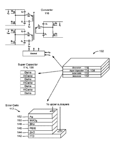
FIGs. 9A and 9B are schematic diagrams showing the physical structures of the
hybrid-
energy device 102 with various energy storages 114 in different embodiments.
In the embodiments shown in FIG. 9A, the hybrid-energy device 102 comprises a
substrate 132 made of one or more suitable transparent or semi-transparent
materials such as glass,
transparent or semi-transparent plastic, transparent or semi-transparent
polymer, and/or the like.
A layer of solar cells 134 are printed, deposited, or otherwise coupled to the
substrate 132. Thus,
the transparent substrate 132 allows the solar cells 112 to expose to ambient
or incident light and
provides support and protection to the solar-cell layer 112 and other layers
thereabove.
In these embodiments, the energy storage 114 comprises a layer of battery
cells 136
printed, deposited, or otherwise coupled to the layer of solar cells 112. A
layer of circuitry of the
multi-input electronic-power converter 116 coupled to the layer of battery
cells 136. The layers of
solar cells 112, battery cells 136, and multi-input electronic-power converter
116 are electrically
connected (not shown) in accordance with FIG. 7 or 8.
The hybrid-energy device 102 in the embodiments shown in FIG. 9B is similar to
that
shown in FIG. 9A except that in these embodiments, the energy storage 114
comprise one or more
capacitors 138 or supercapacitors (i.e., capacitors with large capacitances).
In the embodiments shown in FIGs. 9A and 9B, the solar cells 112 is coated
onto the
substrate 132 followed by the energy-storage layer 114 (being the battery
cells 136 or
supercapacitors 138) and the converter layer 116. In some embodiments as shown
in FIG. 10, the
order of the layers may be the substrate 132, the converter 116, the energy-
storage layer 114 (being
the battery cells 136 in the example shown in FIG. 10), and the solar-cell
layer 112.
In these embodiments, the substrate 132 may comprise a flexible substance such
as PET.
A layer of UV-curable epoxy may be applied on top of the substrate 132 for
protection.
FIG. 11A is a schematic diagram showing the solar-cell layer 112 on a
substrate 132 made
of glass. As shown, the solar-cell layer 112 comprises a plurality of
sublayers such as, naming
from the substrate 132, an anode sublayer 142 made of suitable material such
as Indium Tin Oxide
(ITO) deposited or otherwise coupled onto the substrate 132, a sublayer of
Zinc Oxide (ZnO) 144,
a sublayer of poly(ethylenimine) and poly(ethylenimine) ethoxylated (i.e.,
PEIE) 146, a sublayer
of organic solar-cells 148 such as a sublayer of polymer solar-cells such as a
sublayer of bulk
heterojunctions (BHJs), a sublayer of Molybdenum trioxide (Mo03) 150, and a
cathode
sublayer 152 made of suitable material such as silver (Ag) or Aluminum (Al).
The anode 142 and
the cathode 152 are electrically connected to upper layers such as the energy-
storage layer 114
(i.e., the battery-cell layer 136 or the supercapacitor layer 138) and/or the
integrated-converter
layer 116.
14
CA 03126562 2021-07-13
WO 2020/252584 PCT/CA2020/050848
FIG. 11B is a schematic diagram showing the solar-cell layer 112 on a
substrate 132 made
of a flexible, transparent or semi-transparent material such as a transparent
or semi-transparent
plastic material such as polyethylene terephthalate (PET, also denoted as
poly(ethylene
terephthalate)), poly(ether sulfones) (PES), polyethylene naphthalene (PEN),
polyimide (PI),
and/or the like. The solar-cell layer 112 is the same as that shown in FIG.
11A.
The glass substrate leads to solar cells of rigid structures, whereas the
plastic substrate
results in a flexible solar-cell structure. Those skilled in the art will
appreciate that the plastic
substrate provide many advantages such as:
1) ease of use in large-scale fabrication techniques such as roll-to-roll
coating techniques
for making solar cells and stencil-printing techniques for making batteries;
and
2) flexible solar-cells allowing simplified fabrication process of all layers
thereof
In some embodiments, the solar-cell layer 112, energy-storage layer 114 (i.e.,
battery
layer 136 or capacitor layer 138), and the integrated-converter layer 116 may
be printed in large
scale.
FIG. 12 is a schematic diagram showing the above-described sublayers 142 to
152 of the
solar-cell layer 112 printed in large scale on a substrate 132 to form a
plurality of solar cells. First,
an anode (ITO) sublayer 142 is printed onto the PET substrate 132 as a
plurality of ITO blocks in
a matrix form. Then, a plurality of ZnO sublayers 144 are printed on top of
the ITO sublayer with
each ZnO block 144 coupled to a plurality of ITO blocks 142 in neighboring
rows thereby forming
a parallel connection structure. Then, the PEIE, BHJ, and Mo03, sublayers 146,
148, and 150 are
sequentially printed as a plurality blocks on top of each other. Each set of
PEIE, BHJ, and M003
sublayers 146, 148, and 150 form a solar cell (without counting in the anode
and cathode sublayers)
printed on the anode sublayer 142.
The cathode (Ag or Al) sublayer 152 is finally printed onto the layers stack
as a plurality
of blocks with each cathode block extending to the anode layer 142 of the
neighboring solar cell
such that they are connected in series.
Although in above embodiments, the solar-cell layer 112 comprises a ZnO
sublayer 144
and a PEIE sublayer 146, in some alternative embodiments, the solar-cell layer
112 may comprise
only one of a ZnO sublayer 144 and a PEIE sublayer 146. However, the
performance of the solar-
cell layer 112 in these embodiments may be decreased.
FIG. 13 is a conceptual diagram showing the printing of some sublayers such as
the ZnO,
PEIE, and BHJ sublayers 144, 146, and 148 of the solar-cell layers 112 onto
the substrate 132. In
these embodiments, the M003 and Ag sublayers 150 and 152 are deposited by
using a thermal
evaporator.
CA 03126562 2021-07-13
WO 2020/252584 PCT/CA2020/050848
As shown in FIG. 13, the substrate 132 is arranged on a flat surface of a
platform 172. A
printing device (not shown) with a slot-die head 174 is used for printing the
sublayers/layers. The
slot-die head 174 comprises an ink cartridge 176 filled with respective "ink"
and moves (indicated
by the arrow 178) on the substrate 132 (or a printed layer) to deposit the
material from the ink
cartridge 176 thereto to form solar cells 112 or energy storage cells (not
shown). The solar
cells 112 are first printed onto the substrate 132 and the energy-storage
layer 114 (i.e., battery
cells 136 or supercapacitors 138) are printed onto the solar-cell layer 112.
Then, the multi-input
electronic-power converter 116 (in the form of a printed circuit board) is
coupled to the energy-
storage layer 114.
Herein, the -ink" refers to sublayer/layer material in a suitable form such as
a solution, a
gel, or powder that is used as a precursor for the fabrication of
sublayers/layers. For example, an
ink of ZnO dissolved in butanol may be deposited by slot-die coating for
forming the ZnO
sublayer 144 of the solar-cell layer 112. During the slot-die fabrication of
each sublayer, heat
treatment is usually used for evaporating the solvent to solidify the
fabricated sublayer.
As shown in FIG. 14, in some embodiments, the solar-cell layer 112 may be a
conventional
OPV structure, comprising a plurality of sublayers such as, named from the
substrate 132, a
sublayer of ITO anode 142, a sublayer of poly(3,4-ethylenedioxythiophene)
polystyrene sulfonate
(PEDOT:PSS) 143, a sublayer of BHJs as the active layer 148, and Al or Ag as
the cathode 152.
More organic or inorganic charge transporting layers may also be inserted in
this configuration
for efficient exciton confinement, which would lead to improved performance.
In some embodiments as shown in FIG. 15, the solar-cell layer 112 may comprise
a
plurality of sublayers such as, named from the substrate 132, a fluorine-doped
tin Oxide (FTO)
sublayer 159, an electron-transporting titanium dioxide (TiO2) sublayer 157
deposited directly on
the FTO-coated substrate 132, a pure 2D, a pure 3D, or a mixed 2D-3D hybrid
inorganic-organic
perovskite sublayer 155, a sublayer 153 of 2,2',7,7'-Tetrakis-(N,N-di-4-
methoxyphenylamino)-
9,9'-spirobifluorene (Spiro-OMeTAD) or any other suitable hole-transporting
material which may
be deposited on top of the perovskite sublayer 155, and an Ag or Al deposition
forming a cathode
sublayer 152.
The use of FTO has an advantage of better energy-level alignment between the
work-
function of FTO 159 and the conduction band of TiO2.
In some embodiments as shown in FIG. 16, the solar-cell layer 112 may comprise
a
plurality of sublayers such as, named from the substrate 132, a FTO sublayer
159, a TiO2
sublayer 157, an inorganic quantum-dot (QD) layer 155, a thin Mo03 sublayer
161, followed by
Al, Ag, or gold (Au) electrode 152.
16
CA 03126562 2021-07-13
WO 2020/252584 PCT/CA2020/050848
In these embodiments, both ITO and FTO can be used. Depending on the
conduction band
energy level of the QDs 155, both metal oxides (i.e., ITO and FTO) may provide
a low energy
barrier for efficient charge extraction from the solar cell. Either ZnO or
TiO2 is then deposited
onto the ITO or FTO-coated substrate 132. The active layer 155 is then coated
on the electron-
transporting metal oxide. After that, the fabrication process is completed
with depositing a thin
Mo03 sublayer 161 followed by Al, Ag, or gold (Au) electrode.
In some embodiments as shown in FIG. 17, the solar-cell layer 112 may be a
tandem
structure comprising a perovskite sublayer 171 coupled to a QD solar-cells
layer 175 in series with
an interlayer 173 sandwiched therebetween. The interlayer 173 may be any
suitable organic or
inorganic material. In such a configuration, one of the cells is first
fabricated without depositing
the top metallic electrode. The other cell is then directly fabricated on top
followed by the
deposition of the top electrode. Provided by effective photon harvesting
capabilities of both QD
and perovskite material, efficient and stable tandem solar-cells can be
realized, which may then
be integrated with the other components of the solar-energy harvesting system
100.
In the embodiments shown in FIG. 9B, supercapacitors 138 are used as the
energy-storage
layer 114. FIG. 18 shows the structure of the supercapacitor 138. As shown,
the energy-storage
layer 114 or supercapacitor layer 138 comprises a plurality of Gallium
Arsenide
(GaAs)/Aluminum Gallium Arsenide (AlGaAs) sublayers, such as n AlGaAs layers
(n>0 is an
integer) and (n+1) GaAs layers with each AlGaAs layer sandwiched between two
neighboring
GaAs layers, thereby forming a plurality of semiconductor capacitors.
Each GaAs or AlGaAs sublayer may be deposited by using suitable techniques
such as DC
sputtering, radio-frequency (RF) sputtering, thermal evaporation, and/or the
like.
FIG. 19A is a schematic diagram showing the structure of a battery cell 136 of
the energy-
storage layer 114 in the embodiments shown in FIG. 9A. As shown, the battery
cell 136 comprises
a plurality of sublayers including a pair of current-collector sublayers 202
and 210 coupled to an
anode sublayer 204 and a cathode sublayer 208, respectively, and a separator
sublayer 206
sandwiched between the anode and cathode sublayers 204 and 208.
The electrical current flows through the current-collector sublayers 202 and
210 coupled
to the anode and cathode sublayer sublayers 204 and 208. The anode sublayer
204 is the negative
.. or reducing electrode that releases electrons to the external circuit and
oxidizes during and
electrochemical reaction. The cathode sublayer 208 is the positive or
oxidizing electrode that
acquires electrons from the external circuit and is reduced during the
electrochemical reaction.
The separator sublayer 206 is the medium that prevents short-circuit current
between the
cathode 208 and anode 204 of the battery cell 136 and also provides the ion-
transport mechanism
therebetween. In various embodiments, the separator sublayer 206 may comprise
solid-state
17
CA 03126562 2021-07-13
WO 2020/252584 PCT/CA2020/050848
electrolyte and/or other suitable materials. Compared to the liquid-form
electrolytes which
comprise solvents dissolving salts, acids, or alkalis for ionic conduction and
are usually
flammable, solid-state electrolyte is safer and the resulting battery assembly
may be more compact
as fewer safety-monitoring and/or safety-prevention components and/or
subsystems are needed.
Batteries using solid-state electrolyte also provides improved energy and
power densities.
FIG. 19B is a schematic diagram showing the structure of the battery cell 136
in the form
of a Li-ion battery cell. In this embodiment, each of the current-collector
sublayers 202 and 210
is a thin layer of Aluminum foil or conductive paper. The anode sublayer 204
is activated
Li4Ti5012 (i.e., LTO) with carbon (comprising single-walled carbon nanotubes
(SWCNT) and
carbon powder; described in more detail below) and an electrolyte gel which
comprises a semi-
interpenetrating polymer network (SIPN or semi-1PN) skeleton and Li salt (such
as Lithium
tetrafluoroborate (LiBF4)) dissolved in Sebaconitrile. The separator sublayer
206 is formed by
solid-state electrolyte which in this embodiment is A1203 and the above-
described electrolyte gel.
The cathode sublayer 208 is activated LiCo02 (i.e., Lithium Cobalt Oxide or
LCO) with carbon
(comprising SWCNT and carbon powder; described in more detail below) and the
electrolyte gel.
The Semi-1PN skeleton is an Ultraviolet (UV) curable polymer composed of
ethoxylated
trimethylolpropane triacrylate (i.e., ETPTA) incorporating 1.0 weight percent
(wt%) 2-hydroxy-
2-methylpropiophenone (HMPP) as a photo-initiator and poly(vinylidene
fluoride-co-
hexafluoropropylene) (i.e., PVdF-HFP) with hexafluoropropylene (HFP) content
of 6 mole
percent (mol%) and ETPTA/PVdF-HFP at a ratio of 75/25 weight-by-weight (w/w).
The semi-
IPN skeleton acts as binder for other materials in electrodes and electrolyte.
In order to increase the conductivity of LCO and LTO, the electrode-active LCO
or LTO
powder (e.g., nanoparticles) is coated with SWCNT. Specifically, the LCO or
LTO powder is
added into a SWCNT-suspension solution (LCO/SWCNT at a ratio of 99.75/0.25
w/w,
LTO/SWCNT at a ratio of 99.35/0.65 w/w) and mixed. The mixed solution is then
filtered to
obtain solids which are rinsed and dried to obtain the SWCNT-coated LCO (i.e.,
activated LCO)
or SWCNT-coated LTO (i.e., activated LTO).
An electrode paste for making the cathode sublayer 208 is then formed by
mixing the
SWCNT-coated LCO nanoparticles with carbon black (i.e., carbon powder) and
semi-IPN
skeleton (at a ratio of 55/6/39 w/w/w). An electrode paste for making the
anode sublayer 204 is
then formed by mixing the SWCNT-coated LTO nanoparticles with carbon black
(i.e., carbon
powder) and semi-IPN skeleton (at a ratio of 30/7/63 w/w/w). Herein, carbon
black is used to
increase the conductivity of electrodes.
The solid-state-electrolyte separator sublayer 206 comprises 1 Molar (mol per
liter; M)
LiBF4 in Sebaconitrile (SBN) and semi-IPN skeleton at a ratio of 85/15 w/w,
the aggregation of
18
CA 03126562 2021-07-13
WO 2020/252584 PCT/CA2020/050848
which is then mixed with Al2O3 (about 300 Molar) at a ratio of 60/40 w/w.
A1203 is used as a
spacer to prevent any short-circuit of electrodes.
The battery cell 136 shown in FIG. 19B has many advantages such as being safe
and
flexible compared to the conventional Li-ion batteries that use liquid
electrolyte. On the other
hand, battery cell 136 shown in FIG. 19B also has the disadvantages of complex
manufacturing
(requiring multiple printing-stages) and low anode capacity, and may not be
suitable for large-
scale fabrication.
FIG. 19C is a schematic diagram showing the structure of the battery cell 136
in the form
of a Li-ion battery cell, according to some embodiments of this disclosure. In
this embodiment,
each of the current-collector sublayers 202 and 210 is a thin layer of
Aluminum foil or conductive
paper. The anode sublayer 204 is activated Si comprising SWCNT with graphite
and the above-
described electrolyte gel. The separator layer 206 is a polyethylene or paper-
based nano-porous
material. The cathode sublayer 208 is activated LCO with carbon (comprising
SWCNT and
carbon powder) and the electrolyte gel.
Compared to the battery cell 136 shown in FIG. 19B that uses LTO, the use of
graphite
and Si in these embodiments improves the capacity of battery cell 136.
Compared to using the
Aluminum foil as the current-collector sublayers 202 and 210, using conductive
paper may reduce
the weight of the battery cell 136 and reduce the possible chemical reactions
of the anode 204 and
cathode 208 with the current collectors 202 and 210. Moreover, the usage of
paper-based or
Polypropylene-based (PP) separator makes the fabrication process inexpensive
and facile, and
thus the battery cell 136 in these embodiments is cost-effective for large-
scale fabrications.
The Semi-IPN skeleton is a UV-curable polymer composed of ETPTA incorporating
1.0
wt% HMPP as a photo-initiator. The semi-IPN skeleton acts as a binder for
other materials in
electrodes and electrolyte.
In order to increase the conductivity of LCO and Si, the electrode-active LCO
or Si powder
(e.g., nanoparticles) is coated with SWCNT. Specifically, the LCO or Si powder
is added into a
SWCNT-suspension solution (LCO/SWCNT at a ratio of 99.75/0.25 w/w, Si/SWCNT at
a ratio
of 99.00/1.00 w/w) and mixed. The mixed solution is then filtered to obtain
solids which are rinsed
and dried to obtain the SWCNT-coated LCO (i.e., activated LCO) or SWCNT-coated
Si (i.e.,
activated Si).
An electrode paste for making the cathode sublayer 208 is then formed by
mixing the
SWCNT-coated LCO nanoparticles with carbon black (i.e., carbon powder) and
electrolyte gel (at
a ratio of 55/6/39 w/w/vv). An electrode paste for making the anode sublayer
204 is then formed
by mixing the SWCNT-coated Si nanoparticles with graphite and electrolyte gel
(at a ratio
of 5/45/50 w/w/w). Herein, carbon black is used to increase the conductivity
of electrodes.
19
CA 03126562 2021-07-13
WO 2020/252584 PCT/CA2020/050848
The Nano-porous separator sublayer 206 comprises a nano-porous membrane such
as a
paper membrane, a PP or Polyethylene (PE) based membrane, or the like.
FIG. 20 is a schematic diagram showing two battery cells 136 printed on top of
each other
in series and sharing a common current-collector sublayer (denoted 202/210)
therebetween. Each
battery cell 136 has an output voltage of a volts (V), and the combined
voltage of the two battery
cells 136 is 2a V.
FIG. 21 shows the stencil printing technology for making battery cells 136 by
using a cold
manual laminator as a stencil printer device. In particular, a pair of rollers
222 are rotating as
indicated by the arrows 224 to apply pressure to the hybrid-energy device to
be manufactured
(denoted as 102'; having the substrate 132 and the solar-cell layer 112
printed thereon) which is
fed to the rollers 222 as indicated by the arrows 228. The feeding hybrid-
energy device 102' is
prepared with copper masks (not shown) overlaid thereon and a gel or paste
having the above-
described material of respective one of the sublayers 204 to 208 is applied to
the masked hybrid-
energy device 102'. After passing through the rollers 222, a thin layer 230 of
the gel (with a
.. thickness of about 100 gm) is thus printed or coated onto the masked hybrid-
energy device 102'.
FIG. 22 shows the fabrication process of the anode sublayer 204 on top of the
Aluminum
or conductive-paper current-collector sublayer 202 using the above-described
stencil printing
technique without any processing solvents. As shown, a LTO anode paste 252 is
applied to the
feeding hybrid-energy device 102' having the Aluminum or conductive-paper
current-collector
sublayer 202 (not shown), the rotating rollers 222 apply a pressure onto the
anode paste 252
passing therethrough to form a thin LTO film 204 which is then exposed to UV
irradiation 254
from a Hg UV-lamp 256 with an irradiation peak intensity of approximately 2000
mW.crif2 for
seconds to solidify and form the printed LTO anode sublayer 204.
Then, the hybrid-energy device 102' may be masked and applied with an
electrolyte paste
25 .. and fed through the rollers 222 in a similar stencil-printing and UV-
curing process as described
above to print the solid-state-electrolyte separator sublayer 206 on the anode
sublayer 204. The
cathode sublayer 208 may be then fabricated by printing a cathode paste onto
the solid-state-
electrolyte separator sublayer 206 of the hybrid-energy device 102' and cured
by UV irradiation.
After the Al current-collector sublayer 210 is placed on top of the printed
cathode sublayer 208, a
30 seamlessly integrated all-solid-state battery-cell layer 136 is obtained
which may be a mono full
cell, i.e., the entire batter-cell layer 136 comprising a single battery cell.
The above-described process may be repeated to print another battery-cell
layer 136 on
top, giving rise to printed bipolar battery-cells 136.
In some embodiments, the above-described printing device with the slot-die
head 174
shown in FIG. 13 may be used for printing the sublayers of battery cells 136.
In these
CA 03126562 2021-07-13
WO 2020/252584 PCT/CA2020/050848
embodiments, a specific head 174 may be used for printing all the sublayers of
solid-state battery
cells 136 using slot-die coating. However, stencil printing (see FIG. 21) is
much easier to use with
high-viscosity inks. Moreover, it is not necessary to coat thin (i.e., nm
scale) layers (nm scale) to
fabricate the batteries disclosed herein. The sublayers of battery cells 136
may have relatively
large thickness in ranges of micrometers that may be easily achieved by using
stencil printing.
FIG. 23 shows the details of the hybrid-energy device 102. In this example,
the energy-
storage layer 114 is a supercapacitor layer comprising a plurality of
GaAs/AlGaAs sublayers 138
forming a plurality of semiconductor capacitors as described above.
Integrated Electronic-Power Converter
In some embodiments, the multi-input electronic-power converter 116 may be an
integrated electronic-power converter that may be printed, deposited, or
otherwise integrated to
the layer of battery cells 136 (see FIGs. 9A and 9B). The block diagram of the
integrated
electronic-power converter is shown in FIGs. 24A and 24B show the solar-energy
harvesting
system 100 having an integrated electronic-power converter 116 for AC and DC
applications,
respectively.
FIG. 25A is a block diagram of the integrated electronic-power converter 116.
As shown,
the integrated electronic-power converter 116 comprises a solar-input
converter 284 receiving the
output of the solar-cell layer 112 at a solar input 282 and converting the
solar input 282 to a first
intermediate form (voltage, current, frequency, and/or the like) for
outputting to an output
converter 288. The integrated electronic-power converter 116 also comprises a
battery-input
converter 286 receiving the output of the energy-storage layer 114 at a
battery input 290 and
converting the battery input 290 to a second intermediate form (voltage,
current, frequency, and/or
the like) for outputting to the output converter 288. The output converter 288
receives and
combines the electrical outputs from the solar-input converter 284 and the
battery-input converter
286 and converts the combined electrical energy into a suitable form (voltage,
current, frequency,
and/or the like) for outputting (292) to the load and/or utility grid (not
shown).
In these embodiments, the solar-input converter 284, the battery-input
converter 286, and
the output converter 288 are high-frequency (HF) circuitries and have a
similar functional
structure as shown in FIG. 25B. As can be seen, each of the converters 284,
286, and 288
comprises a power circuit 312 for receiving electricity input which is coupled
to a drive circuit 314
for outputting electricity. A control and sensing module 316 is coupled to the
drive circuit 314 for
controlling the electricity output and for balancing between the solar input
282 and the battery
input 290.
21
CA 03126562 2021-07-13
WO 2020/252584 PCT/CA2020/050848
FIG. 25C is a circuit diagram of the integrated electronic-power converter
116. As shown,
the solar-input converter 284, the battery-input converter 286, and the output
converter 288 are
electrically coupled through a transformer 322 with a ferromagnetic or
ferrimagnetic core. The
control and sensing module 316 senses the output currents ipi and 1p2
(collectively denoted as
with i = 1 or 2) of the solar-input converter 284 and the battery-input
converter 286, respectively,
and the output voltage v, of the output converter 288 and uses I and v, for
adjusting the
parameters of the solar-input converter 284, the battery-input converter 286,
and the output
converter 288 for optimizing the performance thereof.
As shown in FIGs. 26A to 26C, the integrated electronic-power converter 116 in
some
embodiments may be formed by a printed circuitry on a plurality of flexible
printed circuit boards
(PCBs) 330.
In these embodiments, the integrated electronic-power converter 116 is
implemented as an
Integrated Circuit (IC) chip and comprises a core layer 334 made of a ferrite
material thereby
forming a ferrite core. The ferrite core 334 is sandwiched between two silicon-
based wiring
layers 330. FIG. 26C is a schematic perspective view of a portion of the
integrated electronic-
power converter 116. For ease of illustration, the structure of the integrated
electronic-power
converter 116 is shown with gaps between the ferrite core 334 and the wiring
layers 330.
However, those skilled in the art will appreciate that such gaps are for
illustration purposes only
and the actual integrated electronic-power converter 116 may not have any gap
between the ferrite
core 334 and the wiring layers 330. For example, the ferrite core 334 may be
printed, deposited,
or otherwise integrated to either one of the wiring layers 330.
The ferrite core 334 comprises three ferrite loops 336A, 336B, and 336C for
acting as the
cores of the inductors Ls of the solar-input, battery-input, and output
converters 284, 286, and
288, respectively.
The conductive wirings 332 including 332A, 332B, and 332C are distributed on
the wiring
layers 330 and connect the solar-input, battery-input, and output converters
284, 286, and 288. As
shown in FIGs. 26B and 26C, the conductive wirings 332 on the opposite wiring
layers 330 are
connected through vias 342 (conductive holes on the wiring layers 330) and
winding about the
ferrite core 334.
In some embodiments, the integrated electronic-power converter 116 is
implemented as a
circuit board having two wiring layers 220 made of flexible PCBs and a core
layer 334 structured
in a manner similar to that shown in FIGs. 26A to 26C and described above. The
conductive
wirings 332 including 332A, 332B, and 332C are made of etched conductive
layers on the flexible
PCBs 330. The conductive wirings 332 on the opposite flexible PCBs 330 are
connected through
vias 342 and winding about the ferrite core 334.
22
CA 03126562 2021-07-13
WO 2020/252584 PCT/CA2020/050848
Circuits of the Hybrid-Energy Device
FIG. 27 is a circuit diagram showing a DC hybrid-energy device 102 having an
integrated
DC power converter 116DC for powering DC-energy devices (not shown;
collectively denoted as
"output devices") at it output 402, according to some embodiments of this
disclosure. The DC
power converter 116DC may be integrated into the hybrid-energy device 102 and
electrically
connect the solar cells 112 and the energy storage 114 to the respective
output device.
In these embodiments, the integrated DC power converter 116DC comprises a
plurality of
HF circuitry modules including a solar-input converter 284, an energy-storage
converter 286, and
an output converter 288. The integrated DC power converter 116DC also
comprises a current-
shaping control module 316 for precise power-flow control between the solar
cells 112, the energy
storage 114, and the output 402, which shapes the HF currents going through
the HF transformer
332 for achieving desired performance.
As shown in FIG. 27, each of the circuitry modules 284, 286, and 288 comprises
a pair of
power semiconductors such as a pair of metal-oxide-semiconductor field-effect
transistors
(MOSFETs) (Qixv and Q2,pv in the solar-input converter 284, QEEs and Q2,ES in
the energy-storage
converter 286, Qi,. and Q2,0 in the output converter 288) together with a LC
circuit (having two
capacitors and an inductor in this example) for forming a switch circuit for
electrically coupling
through the transformer 322. The circuitry modules 284, 286, and 288 may be
controlled by
adjusting the signals applied to their power-semiconductor gate-terminals
Ql,PV, Q2,PV, OLE% Q2,ES,
Q u, and Q2,o.
In the embodiments shown in FIG. 27, the current-shaping control module 316
senses a
plurality of parameters including the output voltage vpv of the solar-cell
layer 112, the output
voltage of the energy-storage layer 114 vi3t, the output currents ip,PV, ip,ES
of the solar-input
converter 284 and the energy-storage converter 286, respectively (collectively
denoted ip) for
coupling to the output converter 288 via the transformer 322, and the output
voltage v, of the
output converter 288. The current-shaping control module 316 optimizes the
performance of the
integrated DC power converter 116DC by controlling the signals applied to the
power-
semiconductor gate-terminals (collectively denoted Qi,PV, Qi,ES, and Qi,0,
with i = 1 or 2).
In particular, based on the above-described sensed parameters, the current-
shaping control
module 316 controls the gate-terminal signals Qi,PV, Qi,ES, and Qi,0 for
adjusting various signal
parameters such as the duty cycle dpv of the power semiconductors at the
transformer PV-side
284, the duty cycle dEs of the transformer battery-side 286, the duty cycle d0
of the power
semiconductors at the transformer output-side 288, the phase-shift between the
pules for the power
semiconductors at the transformer PV-side 284 and the pulses for the power
semiconductors at
23
CA 03126562 2021-07-13
WO 2020/252584 PCT/CA2020/050848
the output-side 288 (i.e., (ppv), and the phase-shift between the pules for
the power semiconductors
at the transformer battery-side 286 and for the power semiconductors at the
output-side 288 (i.e.
(pEs), and the switching frequency (i.e. Ts), to shape the HF currents of the
three modules 284, 286,
and 288.
FIG. 28 shows the HF waveforms of some signals in the solar-cell module 284.
FIG. 29 is a block diagram of the current-shaping control module 316 for
controlling the
solar-cell module 284 in some embodiments. According to this figure, the power
output from the
solar-cell module 284 is controlled using the phase-shift (ppv between the
pulses of the transformer
PV-side power semiconductors Qi,pv (i = 1, 2) and those of the transformer
output-side power
semiconductors. In particular, the current-shaping control module 316 uses a
constant, reference
current-value as the maximum value for the instantaneous current of the
transformer, and
generates a pair of reference signals v*pv and i*pv for inputting to the
controller 412 (herein, "*"
represents reference signal) which outputs a signal kd,pv. The current-shaping
control module 316
also uses a pair of mono-stable multi-vibrator circuits for detecting the
rising edge of the input
signal Qi,. or Q2,, and outputting a pulse with a predefined duration. Similar
control can be
performed for the energy storage module 286.
Generally, the current-shaping control module 316 determines two signals
/ref], and /rep
respectively at the input sides of the amplifiers 414 and 416 as
ire = 'max ¨ kd,pv X t, when Q2,0 = '1',
1ref2 = 'max ¨ kd,pv X t, when Q1,0 = '1'.
Where "x" represents multiplication.
The signals irqE1 and 1ref2 are then subtracted from Q2,, x I ip,Pv I and Q1,0
x I ip,Pv I "
representing the absolute value of a), respectively, at the amplifiers 414 and
416, and the outputs
of the amplifiers 414 and 416 are used to trigger a S-R flip-flop 418 to
generate the signals Q1.13V
and Q2".
The current-shaping control module 316 for controlling the energy-storage
module 286
may be similar to that shown in FIG. 29, except that the phase-shift may be
positive and negative
depending on the charging or discharging mode of operation.
FIG. 30 shows the waveforms with regards to the current-shaping control module
316. The
controller adjusts the droop slop IQ, (i = 1, 2) of the signals irefi and
iref2 generated by the controller
412 for adjusting the phase-shift and controlling the power. Since the slopes
of the transformer
currents Ip,PV or ip,Es may be positive or negative (depending on the input
and output voltages),
controlling the droop slop may effectively control the phase-shift regardless
of the transformer
current slop. The other control variables such as dpv, d., and T, may be used
to ensure soft-
switching of the power semiconductors.
24
CA 03126562 2021-07-13
WO 2020/252584 PCT/CA2020/050848
FIG. 31 is a block diagram showing the generation of the pulses of the
transformer-
secondary-side power semiconductors by using a Zero Voltage Switching (ZVS)
controlling
circuit 422 which ensures the HF current ip (which may be ippE or ip,Es) to
have correct polarities
at the switching time-instants.
In some embodiments as shown in FIG. 32, a plurality of the DC hybrid-energy
devices 102 (see FIG. 27) may be connected or otherwise combined in parallel
for powering DC
loads 104 and/or a DC grid 118.
In some embodiments as shown in FIG. 33, a plurality of the DC hybrid-energy
devices 102 described herein may be connected or otherwise combined in series
for powering DC
loads 104 and/or a DC grid 118. An advantage of these embodiments is that,
while the voltage
output of each hybrid-energy device 102 may be low, the combination of the
plurality of the
hybrid-energy devices 102 may provide a high-voltage output as needed.
In some embodiments, the DC hybrid-energy devices 102 may be used for powering
AC
loads and/or grids with the use of a DC/AC invertor. For example, FIG. 34
shows a plurality of
the DC hybrid-energy devices 102 connected in parallel for powering DC loads
104 and/or a DC
grid 118 via a single-input DC/AC invertor 432. FIG. 31 shows a plurality of
the DC hybrid-
energy devices 102 connected in series for powering DC loads 104 and/or a DC
grid 118 via a
single-input DC/AC invertor 432.
FIG. 36 is a circuit diagram showing an AC hybrid-energy device 102 having an
integrated
AC power converter 116AC for powering AC-energy devices (not shown;
collectively denoted
output devices) at it output 402, according to some embodiments of this
disclosure. The AC power
converter 116AC may be integrated into the hybrid-energy device 102 and
electrically connect
the solar cells 112 and the energy storage 114 to the respective output
device.
As shown in FIG. 36, the integrated AC power converter 116AC is similar to the
integrated
DC power converter 116DC except that the output converter 288 of the
integrated AC power
converter 116AC further comprises a pair of power semiconductors Q3,o and Q4,0
and an inductor
Lg. Accordingly, the current-shaping control module 316 of the integrated AC
power
converter 116AC also senses the AC output voltage Vg and the AC output current
ig for
optimization. Based on the sensed parameters, the current-shaping control
module 316 also adjusts
the signal applied to the gate terminals of the power semiconductors Q3,0 and
Q4, (i.e., Qi,0 with
i= 1, 2, 3, 4 in FIG. 36).
In these embodiments, the current-shaping control module 316 is similar to
that of the
integrated DC power converter 116DC. For example, the current-shaping control
module 316 for
controlling the solar-cell module 284 may have a structure similar to that
shown in FIG. 29. The
current-shaping control module 316 in these embodiments may also use a ZVS
controlling circuit
CA 03126562 2021-07-13
WO 2020/252584 PCT/CA2020/050848
similar to that shown in FIG. 31 for generating the pulses of the transformer-
secondary-side power
semiconductors and ensuring the HF current ip to have correct polarities at
the switching time-
instants.
Those skilled in the art will appreciate that in some embodiments as shown in
FIG. 37, a
plurality of the AC hybrid-energy devices 102 shown in FIG. 36 may be
connected or otherwise
combined in parallel for powering AC loads 104 and/or an AC grid 106.
Exemplary Use of the Solar-Energy Harvesting System
The above-described solar-energy harvesting system 100 may also be in various
electrical
and electronic devices as a demountable part or as an integrated part thereof
as needed.
For example, FIG. 38 shows a cellphone case 500 having a plurality of
sidewalls 502 and
a rear wall 504 thereby forming a recess 506 for receiving therein a cellphone
(not shown) such
as a smartphone. A hybrid-energy device 102 is integrated on the rear wall 502
thereof As shown
in FIG. 39, the hybrid-energy device 102 comprises, named from the rear wall
502 of the cellphone
case 500, the electronic-power converter 116, the energy storage layer 114,
the solar-cells
layer 112, and a transparent substrate 132 such as a piece of transparent
glass. The energy storage
layer 114 is connected to the batteries in the cellphone via the electronic-
power converter 116.
In some alternative embodiments, the hybrid-energy device 102 may not comprise
the
energy storage layer 114. Rather, the solar-cells layer 112 is connected to
the batteries in the
cellphone via the electronic-power converter 116.
In some alternative embodiments, the case 500 may be a case for other portable
devices
such as a tablet.
In some alternative embodiments, the hybrid-energy device 102 may be
integrated to a
rear wall of a cellphone or a tablet.
In some alternative embodiments, the hybrid-energy device 102 may be
integrated to a
rear wall of the display of a laptop computing device.
In some embodiments as shown in FIG. 40, the hybrid-energy device 102 may be
integrated into the screen 542 of a cellphone 540.
As shown in FIG. 41, the screen 542 comprises, from the outermost layer to the
innermost
layer, a transparent substrate layer 132 such as glass with one or more
sublayers for touch detection
(e.g., capacitive touch detection), a display layer 544 having a plurality of
LEDs for displaying
images thereon, the solar-cells layer 112, the energy storage layer 114, and
the electronic-power
converter 116. The display layer 544 is a transparent layer such as a
transparent OLED layer
allowing light to pass through and reach the solar-cells layer 112 thereunder.
The energy storage
layer 114 is connected to the batteries in the cellphone via the electronic-
power converter 116.
26
A8143242CA
Alternatively, the cellphone 540 may not comprise a separate set of batteries
other than the energy
storage layer 114.
In these embodiments, the cellphone 540 may not comprise the energy storage
layer 114.
Rather, the solar-cells layer 112 is connected to the batteries in the
cellphone 540 via the
electronic-power converter 116.
In various embodiments, the screen 542 may further comprise other necessary
layers
which may be located under the solar-cells layer 112 or, if the layers are
transparent, located above
the solar-cells layer 112.
In some alternative embodiments, the display layer 544 may be a liquid crystal
display
(LCD) layer. In these embodiments, backlight may be required to provide
necessary illumination
for displaying images. Moreover, the light-energy-conversion efficiency of the
solar-cells
layer 112 may be affected by the images displayed on the display layer 544.
For example, the
light-energy-conversion of the solar-cells layer 112 may be significantly
reduced or even disabled
when the display layer 544 displays a dark or a black image thereon.
In some alternative embodiments, the screen 542 may further comprise an
optical-
transformation layer between the transparent substrate 132 and the display
layer 544. The optical-
transformation layer comprises one or more metasurfaces for adjusting one or
more parameters
such as the amplitude or intensity, phase, polarization, pattern, direction,
and the like of the light
emitted from the display layer 544. The detail of the optical-transformation
layer is described in
Applicant's copending US provisional patent application Ser. Nos. 62/862,853,
filed June 18,
2019 and 62/961,317, filed January 15, 2020.
Digital Current Estimation
In the embodiments shown in FIGs. 27 and 29, the current-shaping control
module 316 is
a HF current sensor and comprises necessary sensing circuits (or "sensors")
for sensing a plurality
of parameters. For example, the current-shaping control module 316 uses a HF
current sensor for
sensing the HF current iv.
Current sensors are usually costly and may introduce noise and delay into the
control
module 316. The HF current sensor in the current-shaping control module 316
shown in FIG. 27
and 29 increases the cost of the hybrid-energy apparatus, deteriorates its
power density, and
reduces the reliability of the control module 316.
FIG. 42 shows the current-shaping control module 316 in some embodiments. The
current-
shaping control module 316 in these embodiments similar to that shown in FIG.
27. However, the
current-shaping control module 316 in these embodiments uses a digital HF
current estimator 602
27
Date Recue/Date Received 2021-10-25
CA 03126562 2021-07-13
WO 2020/252584 PCT/CA2020/050848
for estimating the HF current waveform and utilizing it as the feedback for
the closed-loop control
system shown in FIG. 27.
Specifically, the current-shaping control module 316 in these embodiments
receives the
input and output voltages (v0, vBat, vp,) as well as the gate pulse signals
Qi,ES, and to
estimate the HF current waveform, thereby avoiding using any current sensors.
Gallium Nitride (GaN) Gate-Driver Circuit
Prior-art GaN gate drivers may have reliability issues and may not be
appropriate for
industrial applications. One of the main reliability issues stems from the
high reverse conduction
voltage due to the reverse conduction mechanism of GaN devices. In some
embodiments, GaN
devices may be used as the power-semiconductors (Qixv and Q2,PV, QEES and
Q2,ES, and QB. and
Q2.0) in the circuitry modules 284, 286, and 288 of the power converter 116.
In GaN gate-driver circuits, using boot-strap techniques in half-bridge
structures may be
challenging as it requires good regulation of gate bias (e.g., 5-6V bias with
max rating of 7V). As
shown in FIG. 43. during low-side free-wheeling, switch node negative voltage
overcharges
bootstrap capacitors and the high-side gate voltage of the GaN may exceed the
maximum rating
of 7V. As a result, post-regulation or voltage clamping may be required after
bootstrap.
FIG. 44 shows a GaN gate-driver circuit 610 with minimization of the reverse
conduction
time, used in the multi-input electronic-power converter 116. As shown, the
GaN gate-driver
circuit 610 comprises two GaN gates Q1 and Q2 to be charged or discharged. The
GaN gate-driver
circuit 610 uses two control switches Si and S2, a pair of coupled-inductors
Li and L2, a clamp
capacitor CB, and a level-shifter 612 to avoid shoot-through. The level
shifter 612 may be a voltage
source. However, in these embodiments, the level shifter 612 is implemented
using a Zener diode
Dz and a capacitor Cz coupled in parallel and connected to a resistor Rz in
series.
The GaN gate-driver circuit 610 has various advantages such as significant
reduction of
switching losses due to quick turn-on and turn-off of power switch at
transition times, noise
immunity, considerable gate drive loss reduction due to gate energy recovery,
zero-voltage
switching in the drive switches, low number of components, and simplicity of
its control circuit.
Compared to other current-source drivers (CSDs), the GaN gate-driver circuit
610 has a major
advantage, which is that the voltage level of the GaN input capacitance rises
to more than the gate
drive power supply voltage. Parallel inductor may be added to the secondary
side of the
transformer to mitigate the effect of transformer parasitic capacitors.
The enhancement-mode GaN transistor has a property that the device has a
failure
mechanism if the maximum gate voltage for the device exceeds certain voltage
level (e.g., 7V).
This is also true for the depletion-mode GaN device. The enhancement-mode GaN
devices require
28
CA 03126562 2021-07-13
WO 2020/252584 PCT/CA2020/050848
a gate voltage close to certain voltage level (e.g., 6V) to achieve optimal
performance. The
enhancement-mode GaN device, unlike its silicon counterpart, experiences
device failure above
certain voltage (e.g., 7V). When the gate-source voltage of the GaN increases,
the drain-source
resistance in the turn-on status may be lower and result in notable reduction
in conduction loss. In
some high-frequency applications, CSDs with capability to increase the gate-
source voltage of the
GaN device to more than the supply voltage are desirable. The existing gate
drivers for GaN which
is able to drive two GaN in one bridge leg cannot drive the gate with a higher
voltage than the
power supply. The unique feature of the GaN gate-driver circuit 610 is the
boosting capability of
gate-source voltage to lower Rds(on) and, thus, the conduction losses.
With the GaN gate-driver circuit 610, the dead time and consequently reverse
conduction
loss are minimized. In fact, the reason of the reverse conduction loss is the
dead time. In order to
avoid the shoot-through, the dead time may be inserted between the gate-driver
signals. As long
as the crossover level of the gate-driver signals is equal to or less than the
threshold voltage of the
devices, the dead time may be eliminated and the shoot-through may also be
avoided. Because the
crossover level of the gate signals is always at half of Vcc, which is
normally larger than the
threshold voltage, the shoot through problem may incur. In the GaN gate-driver
circuit 610, a level
shifter circuit 612 may be inserted into the driver loop of either the top
switch or the bottom switch.
Based on the level-shift circuit 612, the crossover point may be adjusted to
avoid the shoot-through
problem as shown in FIG. 45. In addition, the negative voltage created by
level-shifter bias ensures
high reliability of the turn-off status to avoid the false tum-on due to the
low threshold voltage.
These benefits make the GaN gate-driver circuit 610 suitable for GaN devices
in half-bridge
structures.
Soft-switching for HF Operations
Soft-switching is important for high frequency applications in order to
significantly reduce
the switching losses. For example, in some embodiments, the electronic-power
converter 116 of
the hybrid-energy device 102 may operate in megahertz (MHz) frequency-range.
Thus, hard
switching may result in excessive switching losses which degrades the
performance and requires
complicated thermal management.
The power converter 116DC shown in FIG. 27 may provide zero-voltage switching
(ZVS)
and substantially decrease the switching losses. However, under certain
conditions, ZVS may be
lost thereby leading to poor performance. This issue stems from the fact that
the high frequency
transformer may have some parasitic capacitances. For example, FIG. 46 shows
various parasitic
capacitances Cpi to Cp3 and Ci to C53 of the HF transformer T. These parasitic
capacitances distort
the ZVS operation under certain conditions.
29
CA 03126562 2021-07-13
WO 2020/252584 PCT/CA2020/050848
FIG. 47 is a circuit diagram of a DC power converter 116DC in some embodiments
which
may be used in the hybrid-energy device 102 shown in FIG. 27. The power
converter 116
comprises a parallel inductor Lp on the output side of the HF transformer 322
for effectively
compensating for the above-described parasitic capacitances and providing soft-
switching for the
DC power converter 116DC. Those skilled in the art will appreciate that a
similar design may be
applied to the AC power converter 116AC shown in FIG. 36.
Thermoelectric Recycling:
Several components of the hybrid-energy device 102 may produce heat. For
instance, solar
panel 112 and power electronics (e.g., the electronic-power converter 116) are
the main sources
of heat in the hybrid-energy device 102.
In some embodiments, the produced heat may be recycled and converted into
electricity
by using a thermoelectric unit (also denoted a "thermoelectric generator"
(TEG)).
FIG. 48 is a schematic diagram showing a thermoelectric unit 620 coupled to a
heat
source 622 such as the solar panel 112 or electronic-power converter 116. The
thermoelectric unit
620 comprises, naming from the heat source 622, a hot plate 624, a
thermoelectric layer 626, and
a cold plate 628.
The hot plate 624 is made of a suitable heat-conductive material such as a
metal material
for receiving heat generated by the heat source 622. In some embodiments, the
hot plate 624 may
be the substrate of the heat source 622. In some other embodiments, the hot
plate 624 may be a
separate plate coupled to the substrate of the heat source 622 using suitable
means such as heat-
conductive glue, screws, bolts, and/or the like. The cold plate 628 is made of
a suitable material
such as metal.
The thermoelectric layer 626 comprises a suitable thermoelectric material with
low heat-
conductivity (or substantially heat nonconductive or heat insulating) and high
electron and hole
mobility (i.e., electrons-and-holes-transportive), such as a two-dimensional
(2D) perovskite or
other suitable 2D materials for converting temperature gradient between the
hot and cold plates
624 and 628 to electrical current. Here, the 2D material is a material that
transports electrons and
holes effectively but has a low heat transfer performance. In these
embodiments, the 2D material
may be any suitable 2D material type and may be different to the 2D
perovskites used in the active
layer of solar cells. A 3D material may transport both electricity and heat,
and thus may not be
preferable in these embodiments.
The hot plate 624, the thermoelectric layer 626, and the cold plate 628 have
good electron
conductivity. Moreover, the thermoelectric layer 626 has a low heat
conductivity, and thus the hot
plate 624, the thermoelectric layer 626, and the cold plate 628 form a
structure for receiving heat
CA 03126562 2021-07-13
WO 2020/252584 PCT/CA2020/050848
from the heat source 622 and trapping the received heat close to the hot plate
624 for converting
it to electricity.
As shown in FIGs. 49A and 49B, the thermoelectric layer 626 in these
embodiments
comprises one or more 2D-material sublayers 632 such as 2D perovskite
sublayers extending
between the hot and cold plates 624 and 628. The one or more 2D-material
sublayers 632 may be
a continuous 2D-material sheet or a plurality of 2D-material sheet-segments or
columns spaced
from each other or separated by a plurality of spacers or fillers such as
membranes 634. For
example, the theimoelectric layer 626 in one embodiment may be made of a
plurality of 2D
perovskite sheets interleaved with a plurality of membrane sheets. In another
embodiment, the
thermoelectric layer 626 may be made by stacking a 2D perovskite sheet with a
membrane sheet
and rolling the stacked sheets to a cylinder to form the thermoelectric layer
626.
In operation, the hot plate 624 receives heat from the heat source 622 and
forms a
temperature gradient in the thermoelectric unit 620 which drives electrons 636
to move towards
the cold plate 628 thereby generating an electrical current.
Thus, the thermoelectric unit 620 may provide useful redundancy for the solar-
energy
harvesting system 100 and may effectively recycle some of the thermal energy
produced by the
heat source 622.
In some embodiments, one of the solar panel 112 or electronic-power converter
116 is
coupled to a thermoelectric unit 620.
In some embodiments, each of the solar panel 112 or electronic-power converter
116 is
coupled to a thermoelectric unit 620.
FIG. 50 shows an exemplary implementation of a PV panel 112 integrated with or
otherwise coupled to a thermoelectric unit or 1EG 620. In this apparatus,
wavelengths of solar
radiation (typically in the range of 300 to 800 nm) are absorbed through the
PV panel 112 and
longer wavelengths are absorbed through the thermoelectric unit 620. By
combining the PV
panel 112 and the TEG 620, the power output thereof is greater than that of
the PV panel 112
alone. Moreover, the TEG 620 also acts as a heatsink which reduces the working
temperature of
the PV panel 112 thereby leading to longer lifetime of the PV panel 112.
FIGs. 51A and 51B are schematic diagrams showing a photovoltaic-thermoelectric
unit 650, according to some embodiments of this disclosure. As shown, the
photovoltaic-
thermoelectric unit 650 comprises a light-harvesting layer 652 and a TEG 620
coupled thereto.
The TEG 620 is similar to that shown in FIGs. 48 to 50 and comprises, naming
from the light-
harvesting layer 652, a hot plate 624, a thermoelectric layer 626, and a cold
plate 628.
The light-harvesting layer 652 comprises a first sublayer having a plurality
of solar
cells 654 mixed with a plurality of metasurfaces 656 (which are a plurality of
nano-columns as
31
CA 03126562 2021-07-13
WO 2020/252584 PCT/CA2020/050848
shown in FIG. 47C), and a second sublayer having a plurality of nano-wires 658
coupled to the
first sublayer.
As those skilled in the art will appreciate, solar cells 654 can only harvest
energy in a
specific frequency spectrum. In conventional solar panels, the unharvested
optical energy is
usually wasted as heat.
In these embodiments, the metasurfaces 656 are designed to utilize the energy
of the light
spectrum that is unusable by the solar cells 654 to further improve the solar-
energy usage.
Specifically, the metasurfaces 656 may be designed to conduct light with
certain frequencies such
as those unusable by the solar cells 654. This light conducted through the
metasurfaces 656 are
converted to heat by the nano-wires 658 and then converted into electricity by
the TEG 620.
As shown in FIG. 51D, the nano-wires 658 may be embedded in the hot plate 624
and
directly transfer the converted heat to the thermoelectric layer 626 for
converting to electricity.
FIG. 52 shows a thermoelectric unit or TEG 700 according to some embodiments
of this
disclosure. In these embodiments, the TEG 700 comprises a hot plate 624 and a
cold plate 628
similar to those described above, and a nano-channel layer 702 sandwiched
between the hot and
cold plates 624 and 628. The nano-channel layer 702 comprises a plurality of
nano-channels 704
in parallel. The nano-channels are made of suitable electrically conductive
material such as carbon
(e.g., graphene), gold, and/or the like, and have one or more subwavelength
dimensions. For
example, in some embodiments, the nano-channel layer 702 may have a
subwavelength thickness
(the dimension between the hot and cold plates 624 and 628) such as about 10
nm to allow
quantum effect to be prominent for moving electrons (see FIG. 49B).
In these embodiments, the nano-channels 704 are used for trapping the heat in
the hot-
plate side and providing a channel for electrons 706 to flow therethrough. In
other words, the
nano-channel laver 702 is electrically conductive to allow electrons 706 flow,
but on the other
hand impedes the heat-transfer and maintains temperature gradient.
In some similar embodiments, the nano-channel layer 702 may comprise a
plurality of
nano-channels 704 arranged in series or in a mixture of parallel and series;
see FIG. 53.
Supercapacitor Technology
Energy storage in the solar-energy harvesting system 100 is important as the
solar light
conditions in practice are usually unstable. Considering the intermittency of
the solar energy, the
energy storage unit may be an integral part of the hybrid-energy device 102.
Various methods may be used to store energy, among which batteries and
supercapacitors
are the most common solutions because of their superior performance. For
example, in some
embodiments, high-density Lithium-Ion (LI) batteries may be used for storing
energy.
32
CA 03126562 2021-07-13
WO 2020/252584 PCT/CA2020/050848
In some embodiments, such as in embodiments where PV panels 112 having large
sizes
are used, supercapacitors may be used for storing energy.
Supercapacitors are a relatively new class of energy storage systems that have
fast power
delivery and life-time of more than thousands of charge-discharge cycles at
high current densities.
Electrochemical double layer capacitors (EDLCs) store opposite charges at the
interface of anode
and cathode by physisorption which is a different mechanism compared to
batteries (energy
storage occurs by means of redox reactions). As a result, supercapacitors can
offer faster ion-
exchange kinetics and longer working cycles compared to batteries.
Supercapacitors specifically
appealing to be used in high power applications such as hybrid electrical
vehicles and power
station.
FIGs. 54A and 54B show the structure of a supercapacitor 740. As shown the
supercapacitor 740 comprises a plurality of stacked capacitor layers 742
coupled to a pair of
conductors or electrical terminals 744 and 746.
Each capacitor layer 742 comprises a pair of thin-film sublayers 752
sandwiching and
separated by an electrically insulating membrane sublayer 754 therebetween,
and a pair of
conductor sublayers 756 and 758 sandwiching the thin-film sublayers 752 (and
the membrane
sublayer 754) therebetween. The thin-film sublayers 752 are made of
electrically conductive thin-
film materials such as a mixture of activated carbon, graphene, graphite,
and/or the like. The
membrane sublayer 754 is coated with ionic liquid material, or by soaking the
membrane in the
ionic liquid and removing the excess liquid by hanging the membrane for a few
minutes.
Each of the conductor sublayers 756 and 758 is electrically connected to a
respective
terminal 744 or 746. For example, as shown in FIG. 54A, the conductor sublayer
756 is electrically
connected to the terminal 744 and the conductor sublayer 758 is electrically
connected to the
terminal 746.
When a plurality of capacitor layers 742 are stacked together, neighboring
capacitor
layers 742 may share a conductor sublayer. For example, as shown in FIG. 54A,
the neighboring
capacitor layers 742-1 and 742-2 share a conductor sublayer 762 which is
effectively the
conductor sublayer 758-1 of the capacitor layer 742-1 and the conductor
sublayer 758-2 of the
capacitor layer 742-2. Similarly, the neighboring capacitor layers 742-2 and
742-3 share a
conductor sublayer 764, and the neighboring capacitor layers 742-3 and 742-4
(not shown) share
a conductor sublayer 766.
With this structure. the supercapacitor 740 may have a thin thickness with a
large area. A
plurality of supercapacitors 740 may be integrated to provide sufficient
storage capacity required
for the hybrid-energy device 102. The supercapacitor 740 has several major
advantages.
33
CA 03126562 2021-07-13
WO 2020/252584 PCT/CA2020/050848
For example, the use of thin-film materials facilitates the building of high
energy-density
supercapacitors 740.
The supercapacitor 740 has a fast dynamic behavior, i.e., charging and
discharging of the
supercapacitor 740 may be much faster than that of batteries. Such a fast
dynamic behavior is
important to the solar-energy harvesting system 100 due to the erratic nature
of the solar energy.
Another advantage of the supercapacitor 740 is its lifetime. Unlike batteries,
there is no
electrochemical reactions in the supercapacitor 740. Thus, the lifespan of the
supercapacitor 740
may be extended many years with minimal performance degradation.
Yet another advantage of the supercapacitor 740 is its wide temperature range
which
makes it ideal for outdoor applications.
In the following a symmetric supercapacitor and a fabrication process thereof
are described.
The supercapacitor may comprise one or more supercapacitor cells with each
supercapacitor cell
comprising a separator such as a membrane, electrolyte (i.e., ionic liquid), a
cathode, an anode,
and a pair of current collectors.
In some embodiments the membrane may be cellulose fiber. In some other
embodiments,
the membrane may be a polymer membrane with high density of pores and/or a
suitable separator
offered by Celgard LLC of Charlotte, North Carolina, United States.
The electrolyte ionic liquid may be 1-Ethyl-3-methylimidazolium
tetrafluoroborate
(EMIMBF4) which is air and water stable thereby making it a good candidate for
supercapacitors
working at extreme hot or cold temperatures.
The cathode and anode may comprise thin films of conductive material coated on
the
surface of the separator.
In some embodiments, silver nanoparticles dissolved in xylene or other
suitable solvents
may be used for forming the current collector. In some other embodiments a
thin foil of metal or
graphene-based sheet may be used as the current collector. In still some other
embodiments, a
combination of coated silver ink and thin foil may be used for forming the
current collector.
Each supercapacitor cell may be formed by a membrane coated with ionic liquid,
conductive ink, and current collector. The conductive ink may comprise
activated carbon,
graphene, binder, and volatile solvent. In some embodiments, both cathode and
anode can be
fabricated using the same conductive ink and in other embodiments the
components in the ink can
be different for electrodes.
The supercapacitor cells may be fabricated using a suitable printing or
coating technology
such as a combination of slot-die coating, spray coating printing, and doctor
blade. The ink used
to print the cathode and anode comprises activated carbon, graphene, carbon
nanotube, and binder
dispersed in a volatile solvents such as acetone.
34
CA 03126562 2021-07-13
WO 2020/252584 PCT/CA2020/050848
FIG. 55 shows the structure of a supercapacitor 800, according to some
embodiments of
this disclosure. The supercapacitor 800 in these embodiments is a symmetric
supercapacitor
having an anode 802 and a cathode 804 separated by a membrane 806, and a pair
of current
collectors 808 and 810 sandwiching the combination of the anode 802, membrane
806, and
cathode 804 therebetween. The supercapacitor 800 also comprises ionic liquid
(not shown)
between the anode 802 and membrane 806, and between the cathode 804 and
membrane 806.
In these embodiments, the anode 802, cathode 804, and the current collectors
808 and 810
are coated films coated with a suitable conductive material. The membrane 806
may be a cellulose
or polymer with high rate of porosity. The ionic liquid may be EMIMBF4 or
similar electrolytes.
The cathode and anode are made of similar material with sufficient electrical
conductivity.
With this structure, the supercapacitor 800 is a flexible supercapacitor.
In some embodiments, the supercapacitor 800 may be fonned by one or more
supercapacitor cells 800' wherein each supercapacitor cell 800' has a
structure as shown in
FIG. 55.
FIG. 56 is a schematic diagram showing a fabrication process 820 of the
supercapacitor
cells 800' using a spray-coating technology. The fabrication process 820 is
suitable for large-scale
fabrication of supercapacitor cells 800'.
In various embodiments, the slot-die coater or doctor blade methods may be
used as a
printing tool. In some embodiments, in addition to the spray-coated current
collector, a thin foil
of metal or GRAFOIL flexible graphite (GRAFOIL is a registered trademark of
Neograf
Solutions, LLC of Lakewood, Ohio, USA) may be used to reduce the resistivity
of the cell. The
thin foil of metal may be aluminum, nickel or other materials depending on the
choice of ionic
liquid and conductive ink compound. In some embodiments, PMMA may be used as
an insulator
and encapsulant.
In these embodiments, the ink compound has high concentration of activated
carbon and
graphene mixed with stabilizer and volatile solvents to facilitate the
fabrication process 820. In
some embodiments, the ink may be made of carbon nanotubes or carbon fiber
mixed with
activated carbon and graphene. In some embodiments supercapacitor cells 800'
may be fabricated
using different cathode and anode materials or different concentration of
compounds in the ink.
As shown in FIG. 56, at the ink preparation stage 822, the conductive ink is
processed
using a ball mill 842 to crush down the material 844 therein such as activated
carbon, graphene,
binder, and suitable medium, to fine-size particles. All the powders and
solvents are added in this
step to the ball mill and let it mix for few hours. The processed ink is then
filtered and transferred
to the printing station (not shown).
CA 03126562 2021-07-13
WO 2020/252584 PCT/CA2020/050848
At the coating stage 824, two spray coaters 846 are used to sequentially apply
the
solutions 848 of ionic liquid, conductive ink, and current collector onto the
opposite sides of the
membrane 806 with proper annealing procedure to remove the volatile solvents.
Al the encapsulation stage 826, two spray coolers 856 are used to apply a thin
layer of
PMMA insulator 858 onto the supercapacitor cell 800' to prevent short-circuit
of stacked
supercapacitor cells. At the packaging stage 828, the supercapacitor cells
800' are transferred to a
vacuum chamber for final encapsulation and packaging for making the
supercapacitors 800.
FIG. 57 shows a supercapacitor 800 formed by stacking a plurality of
supercapacitor cells 800' with suitable insulators 872 such as PMMA insulators
sandwiched
between each pair of neighboring supercapacitor cells 800' for electrical
insulation. In these
embodiments, the supercapacitor cells 800' may be stacked in series or in
parallel. The PMMA
insulators may be coated to the supercapacitor cells 800'.
With this structure, the supercapacitor 800 may have extended lifetime of each
cell 800'
as PMMA is a good encapsulation material which prevents air and moisture from
entering the
supercapacitor cells 800'.
Although embodiments have been described above with reference to the
accompanying
drawings, those of skill in the art will appreciate that variations and
modifications may be made
without departing from the scope thereof as defined by the appended claims.
36