Note : Les descriptions sont présentées dans la langue officielle dans laquelle elles ont été soumises.
CA 03122600 2021-06-09
A8142819WO
LIGHT-EMITTING APPARATUS USING METASURFACES AND LIGHT-EMITTING
METHOD THEREOF
CROSS-REFERENCE TO RELATED APPLICATIONS
This application claims the benefit of US Provisional Patent Application
Serial Nos.
62/862,853, filed June 18, 2019 and 62/961,317, filed January 15, 2020.
FIELD OF THE DISCLOSURE
The present disclosure relates to light-emitting methods, apparatuses, and
systems, and in
particular to light-emitting methods, apparatuses, and systems using
metasurfaces for controlling
the emitted lights.
BACKGROUND
Light-Emitting Diodes (LEDs) are known and have been widely used in many
industries,
mostly as low-power light indicators. In recent years, LEDs with increased
power output or
increased luminous intensity have been developed and used as the light source
for illumination.
For example, with improved energy efficiency, safety, and reliability, LED
lights are replacing
other types of lights in the market such as incandescent lights, Compact
Fluorescent Lamps (CFLs),
and the like. As everyday lighting significantly contributes to the burden on
power grids and
greatly increases the overall requirements for electricity generation, the
energy efficiency of LEDs
will play a crucial role in future energy savings. It is likely that LEDs will
dominate the lighting
markets because of their superior energy efficiency.
High-efficient LEDs have been replacing the conventional lighting solutions in
a variety
of applications such as flashlights, portable lights, lamps, streetlights, and
the like. LEDs may be
powered by various types of power sources such as batteries, conventional
power grids, renewable
energy systems and energy storage systems e.g. systems using photovoltaic (PV)
panels and
battery banks, and the like, thereby providing great flexibility in adapting
lighting solutions to
specific use scenarios.
In many lighting solutions, it may be preferable to configure the light source
such as a
LED light source to emit directional light, e.g., to form a convergent beam
and focus onto a
predefined area for obtaining an enhanced illumination intensity, to form a
collimated beam for
reaching a target at distance, to form a divergent beam for illuminating a
large area, and/or the
like. In some lighting solutions, the light direction of the light source may
be preferably adjustable.
In prior art, light sources usually use mirrors or reflective surfaces for
forming directional light,
1
Date Recue/Date Received 2021-06-09
CA 03122600 2021-06-09
WO 2020/252585
PCT/CA2020/050849
and mechanical means are often used for turning the mirrors or reflective
surfaces to adjust the
light direction. Such directional-lighting means are usually of relatively
large size, slow
responsive, and less efficient.
LEDs with increased power output and/or increased luminous intensity have also
been
used as light sources for growing plants and the like. Such LEDs, which are
sometimes called
LED grow lights, provide various advantages such as producing precise
wavelengths of lights,
high intensity, high efficiency, and the like. LED grow lights are also
advantageous for indoor
plant growing as the process of growing plants can be performed in controlled
environments with
much less risks and other unwanted outdoor variables.
The plant growth occurs as a result of -photosynthesis" processes. As known in
the art,
the photosynthesis processes convert carbon dioxide (CO2) into organic
materials using energy
from the light. Specifically, the optical energy is absorbed through special
proteins containing
chlorophyll pigments that exist in photosynthetic cell membranes called
chloroplasts. The
photosynthetic cells are mainly in plant leaves.
However, chlorophyll only absorbs energy from particular parts or colors of
the light
spectrum. The effective spectra are across the blue and red color spectra. The
green part of the
light spectrum is reflected, which is why plant leaves are usually in green
color. When
photosynthetic cells in leaves die and the chlorophyll is degraded, other
pigmented molecules in
the leaves dominate light reflection while they are degraded to the point
where the leaves only
exhibit brown colors.
Thus, it is known that different pigments in chloroplasts absorb specific
wavelengths of
light to contribute to photosynthesis, and the photosynthetic efficiency or
rate has strong
correlation with the spectrum of illumination.
For example, rice plants grown under blue and red illumination have higher
photosynthesis
efficiency than those grown under only red illumination. Pea leaves grown
under red LED light
contain higher levels of 13-carotene than those grown under blue or white LED
light.
Light intensity is another influential factor in photosynthesis due to the
response of
photosynthesis organisms to high-light intensity to reduce stress effects.
Under red LED light,
wheat seedlings accumulate chlorophyll at 100 mot m-2 s-1-, but not at 500
pmol m-2 s-1.
It is observed that plants usually absorb the blue light spectra during their
early growth,
and then increasingly absorb the red light spectra as they mature and during
their blooming phase.
It is also observed that some plants have highly ordered constituents that
make their interactions
with light polarization sensitive. For example, such plants may more
efficiently absorb or reflect
light with a specific polarization state than light with other polarization
states.
2
CA 03122600 2021-06-09
WO 2020/252585
PCT/CA2020/050849
In addition, plants are capable of sensing duration of lighting period and
time, and change
their growth rates accordingly.
Plant cultivation using constant or universally defined illumination
configuration is neither
energy efficient nor optimal for photosynthesis. As prior-art LED grow lights
usually provide light
for the plants without consideration for the aforementioned factors, they fail
to provide optimized
lighting configurations for optimizing the physiological processes of growing
plants. Moreover,
different plants require different light characteristics (for example,
intensity, spectrum,
polarization, time, and the like) to achieve the best growth performance.
However, prior-art LED
grow lights fail to adapt to the plant needs and fail to provide appropriate
light characteristics.
For example, conventional illumination systems such as LED panels used for
indoor plant
growth usually do not produce a uniform distribution of light over the plants.
They often have
intensities strongest at the center and increasingly diminishing away from the
center.
FIG. 1A shows a conventional light source 10 emitting a light beam 12 towards
a square
image plane 14 at a distance thereto. FIG. 1B shows the light-intensity
distribution 16 on the image
plane 14. As can be seen, the conventional light source 10 does not produce a
uniform distribution
of light on the image plane 14. Rather, the light-intensity distribution 16 on
the image plane 14 is
strongest at the center thereof and gradually diminishing away from the
center. Moreover, the
intensity light distribution 16 is symmetric about the incidence point of the
light beam 12 on image
plane 14.
FIGs. 2A and 2B show the illumination pattern that an LED panel 10 produces in
a 6x6
square-meters (m2) image plane 14 about 3 meters (m) away from the panel 10,
obtained using
ray-tracing. The intensity distribution is clearly non-uniform.
Therefore, a grow light using such a light source 10 that provides sufficient
light in the
plant periphery would cause over-illumination at the center of the plant
thereby leading to poor
plant growth. On the other hand, providing sufficient lighting in the plant
center would cause
inefficient lighting at the plant periphery, also leading to poor plant
growth. Such an intensity
distribution is due to symmetry of the image plane center with respect to the
light emitters.
Such a light source 10 may not be desirable in other applications. For
example, a street
light using such a light source 10 may cause glares and overall inefficient
illumination.
LEDs are also used for indoor and outdoor displays which also require
deliberate control
of various light characteristics such as intensity, polarization, time, and/or
the like with fast
response.
Therefore, it is always a desire for a LED apparatus, system, and method with
controlled
light characteristics.
3
CA 03122600 2021-06-09
WO 2020/252585
PCT/CA2020/050849
SUMMARY
According to one aspect of this disclosure, there is provided a light-emitting
apparatus.
The light-emitting apparatus comprises: a light-emitting layer for emitting
light; and an optical-
transformation layer coupled to the light-emitting layer, the optical-
transformation layer
comprising one or more optical-transformation units, each optical-
transformation unit comprising
a metasurface for adjusting one or more parameters of the light emitted from
the light-emitting
layer.
In some embodiments, the light-emitting layer comprises one or more Light-
Emitting
Diodes (LEDs) for emitting light.
In some embodiments, the optical-transformation layer is printed onto the
light-emitting
layer.
In some embodiments, the light-emitting layer comprises one or more light-
emitting units;
the optical-transformation layer comprises a housing having one or more
receptacles for receiving
the one or more metasurfaces; and the one or more receptacles are at locations
corresponding to
those of the one or more light-emitting units for aligning the one or more
metasurfaces with the
one or more light-emitting units.
In some embodiments, each of the one or more receptacles comprises an
outwardly
expanding inner surface having an inner opening for receiving light emitted
from the light-
emitting layer and an outer opening for passing through the received light,
the outer opening
having an area greater than that of the inner opening.
In some embodiments, the inner surface of each of the one or more receptacles
is reflective.
In some embodiments, the cross-section of the inner surface of each of the one
or more
receptacles has a paraboloid shape.
According to one aspect of this disclosure, there is provided a light-emitting
apparatus.
The light-emitting apparatus comprises: a light-emitting layer for emitting
light: and an optical-
transformation layer comprising one or more optical-transformation units, each
optical-
transformation unit comprising a metasurface, at least one metasurface being
polarization-
selective for selectively passing therethrough the hula emitted from the light-
emitting layer with
a predefined polarization state.
In some embodiments, each of the one or more metasurfaces comprises a
plurality of nano-
scale structures arranged in an asymmetric base geometry.
In some embodiments, the light-emitting apparatus further comprises a
polarization-
control layer sandwiched between the light-emitting layer and the optical-
transformation layer for
polarizing the light emitted from the light-emitting layer.
4
CA 03122600 2021-06-09
WO 2020/252585 PCT/CA2020/050849
In some embodiments, the light-emitting apparatus is a grow light for
facilitating the
growth of one or more plants.
According to one aspect of this disclosure, there is provided alight-emitting
apparatus for
facilitating the growth of one or more plants. The light-emitting apparatus
comprises: a light-
emitting layer for emitting light; and at least one optical-transformation
layer comprising one or
more optical-transformation units, each optical-transformation unit comprising
a metasurface for
adjusting one or more parameters of the light emitted from the light-emitting
layer for optimizing
illumination configurations of the one or more plants.
According to one aspect of this disclosure, there is provided a display
apparatus. The
display apparatus comprises: a light-emitting layer for emitting light; and at
least one optical-
transformation layer comprising one or more optical-transformation units, each
optical-
transformation unit comprising a metasurface for adjusting one or more
parameters of the light
emitted from the light-emitting layer for displaying one or more images.
According to one aspect of this disclosure, there is provided a light-emitting
apparatus.
The light-emitting apparatus comprises: a light-emitting layer for emitting
light; a polarization-
control layer coupled to the light-emitting layer for polarizing the light
emitted from the light-
emitting layer; and at least one optical-transformation layer coupled to the
polarization-control
layer, the at least one optical-transformation layer comprising one or more
optical-transformation
units, each optical-transformation unit comprising at least one metasurface,
at least one
metasurface being polarization-selective for selectively passing therethrough
the polarized light
from the polarization-control layer for switching between different
illumination patterns or images.
According to one aspect of this disclosure, there is provided a light-emitting
apparatus.
The light-emitting apparatus comprises: a light-emitting laver for emitting
light; a polarization-
control layer coupled to the light-emitting layer for polarizing the light
emitted from the light-
emitting layer; and at least one optical-transformation layer coupled to the
polarization-control
layer, the at least one optical-transformation layer comprising one or more
optical-transformation
units, each optical-transformation unit comprising at least one metasurface,
at least one
metasurface being polarization-selective for selectively passing therethrough
the polarized light
from the polarization-control layer for creating multiple different
illumination patterns or images
at different locations.
According to one aspect of this disclosure, there is provided a light-emitting
apparatus.
The light-emitting apparatus comprises: a light-emitting layer for emitting
light towards a source
field of view (FOV); and at least one metasurface layer in front of the light-
emitting layer for
directing the light emitted from the light-emitting layer towards a first FOV
having an angular
span smaller than that of the source FOV.
5
CA 03122600 2021-06-09
WO 2020/252585
PCT/CA2020/050849
In some embodiments, the light-emitting apparatus further comprises a
polarization-
control layer sandwiched between the light-emitting layer and the at least one
optical-
transformation layer; the polarization-control layer is configured for, in
response to a control
signal, polarizing the light emitted from the light-emitting layer to a first
polarization state or to a
second polarization state; and wherein the at least one optical-transformation
layer is configured
for directing the light from the polarization-control layer in the first
polarization state towards a
first FOV having an angular span smaller than that of the source FOV, and
directing the light from
the polarization-control layer in the second polarization state towards a
second FOV having an
angular span greater than that of the first FOV.
According to one aspect of this disclosure, there is provided a light-emitting
apparatus.
The light-emitting apparatus comprises: a light-emitting layer for emitting
light; and an optical-
transformation layer in front of the light-emitting layer, the optical-
transformation layer
comprising a plurality of optical-transformation units, each optical-
transformation unit comprising
a metasurface for directing light emitted from the light-emitting layer
towards a target area for
forming a predefined light-distribution pattern.
In some embodiments, the predefined light-distribution pattern is a
substantively uniform
optical-energy distribution on the target area.
In some embodiments, the plurality of metasurfaces comprise a first set of
metasurfaces
for directing the light emitted from the light-emitting layer towards borders
of the target area, and
a second set of metasurfaces for directing the light emitted from the light-
emitting layer towards
a center of the target area, for generating the substantively uniform optical-
energy distribution on
the target area.
According to one aspect of this disclosure, there is provided a solar-energy
harvesting
apparatus. The solar-energy harvesting apparatus comprises: a photovoltaic
layer having a
plurality of photovoltaic cells; and at least one metasurface layer in front
of the photovoltaic layer
for directing light to the photovoltaic layer substantively without causing
reflection on the
photovoltaic layer.
In some embodiments, the solar-energy harvesting apparatus comprises a
plurality of
metasurface layers for directing light at an incident angle within a
predefined range to
perpendicularly imping the photovoltaic layer.
According to one aspect of this disclosure, there is provided a light-emitting
apparatus.
The light-emitting apparatus comprises: a light-emitting layer for emitting
light; and at least one
metasurface layer in front of the light-emitting layer for directing the light
emitted from the light-
emitting layer in a first polarization state towards a first FOV and directing
the light emitted from
.. the light-emitting layer in a second polarization state towards a second
FOV; the first and second
6
CA 03122600 2021-06-09
WO 2020/252585
PCT/CA2020/050849
FOVs are overlapped and laterally offset from each other for forming a three-
dimensional (3D)
perception to a user wearing a pair of glasses with lenses of different
polarization states.
According to one aspect of this disclosure, there is provided a light-emitting
apparatus.
The light-emitting apparatus comprises: a light-emitting layer for emitting
light; and at least one
metasurface layer in front of the light-emitting layer for directing the light
emitted from the light-
emitting layer in a first polarization state towards a first FOV and directing
the light emitted from
the light-emitting layer in a second polarization state towards a second FOV;
the first and second
FOVs are laterally offset from each other such that the first FOV is only
viewable to a first eye of
a user at a predefined distance and the second FOV is only viewable to a
second eye of the user at
.. the predefined distance, for forming a 3D perception to the user.
BRIEF DESCRIPTION OF THE DRAWINGS
FIG. 1A is a schematic diagram showing a prior-art light source emitting a
light
beam towards a square image plane at a distance thereto;
FIG. 1B shows the light-intensity distribution on the image plane of the light
emitted from
the prior-art light source shown in FIG. 1A;
FIG. 2A is a schematic diagram showing a prior-art Light-Emitting Diode (LED)
panel
emitting a light beam towards a square image plane at a distance thereto;
FIG. 2B shows the illumination pattern on the image plane of the light emitted
from the
prior-art LED panel, obtained using ray-tracing;
FIG. 3 is a schematic diagram showing the structure of a lighting-emitting
apparatus,
according to some embodiments of this disclosure, the lighting-emitting
apparatus comprising a
LED light-emitting layer and an optical-transformation layer having one or
more metasurfaces;
FIG. 4 is a schematic exploded view of the lighting-emitting apparatus shown
in FIG. 3;
FIG. 5 shows an optical-transformation unit of an optical-transformation layer
of the
lighting-emitting apparatus shown in FIG. 3;
FIG. 6 shows an example of the structure of a metasurface for forming the
optical-
transformation unit shown in FIG. 5;
FIG. 7 is a schematic exploded view of a lighting-emitting apparatus,
according to some
embodiments of this disclosure, the lighting-emitting apparatus comprising a
LED light-emitting
layer, a polarization-control layer, and a metasurface optical-transformation
layer;
FIG. 8A is a schematic diagram showing a pixel of the polarization-control
layer of the
light apparatus shown in FIG. 7, according to some embodiments of this
disclosure;
7
CA 03122600 2021-06-09
WO 2020/252585
PCT/CA2020/050849
FIG. 8B is a schematic diagram showing a pixel of the optical-transformation
layer of the
light apparatus shown in FIG. 7, corresponding to the pixel of the
polarization-control layer shown
in FIG. 8A;
FIG. 9A is a schematic diagram showing a pixel of the polarization-control
layer of the
light apparatus shown in FIG. 7, according to yet some embodiments of this
disclosure;
FIG. 9B is a schematic diagram showing a pixel of the optical-transformation
layer of the
light apparatus shown in FIG. 7, corresponding to the pixel of the
polarization-control layer shown
in FIG. 9A;
FIG. 10A is a schematic diagram showing a pixel of the polarization-control
layer of the
light apparatus shown in FIG. 7, according to still some embodiments of this
disclosure;
FIG. 10B is a schematic diagram showing a pixel of the optical-transformation
layer of the
light apparatus shown in FIG. 7, corresponding to the pixel of the
polarization-control layer shown
in FIG. 10A;
FIGs. 11A and 11B are schematic diagrams showing the light apparatus shown in
FIG. 7
displaying two images at two directions, according to the embodiments shown in
FIGs. 8A and
8B, or FIGs. 9A and 9B;
FIG. 12 is a schematic diagram showing the light apparatus shown in FIG. 7
displaying
two images at two directions, according to the embodiments shown in FIGs. 8A
and 8B, FIGs. 9A
and 9B, or FIGs. 10A and 10B;
FIG. 13 is a schematic exploded view of a lighting-emitting apparatus haying a
plurality
of fiber-optic cables, according to some embodiments of this disclosure;
FIG. 14 is a conceptual diagram showing the printing of the optical-
transformation laver
of the lighting-emitting apparatus shown in FIG. 3;
FIG. 15 is a schematic diagram of a lighting system for facilitating the
growth of plants,
according to some embodiments of this disclosure;
FIG. 16 is a schematic diagram of a lighting system for facilitating the
growth of plants,
according to some embodiments of this disclosure, the lighting system
comprising a sensor for
monitoring the growth of the plants;
FIG. 17 is a schematic diagram showing the structure of a solar-cells layer
incorporated in
the lighting-emitting apparatus shown in FIG. 3;
FIG. 18 is a schematic diagram showing the structure of a lighting system for
use as an
illumination or light source with controlled illumination patterns, according
to some embodiments
of this disclosure;
FIG. 19 illustrates an example of forming a cost function used by the lighting
system
shown in FIG. 18 for generating an illumination pattern;
8
CA 03122600 2021-06-09
WO 2020/252585
PCT/CA2020/050849
FIG. 20 is a flowchart showing the steps of a process executed by a processing
structure
of the lighting system shown in FIG. 18 for finding the global (or near-
global) minimum of the
cost function using a gradient descent method;
FIGs. 21 to 25 show the optimization results of the process shown in FIG. 20
for generating
various illumination patterns;
FIG. 26 is a schematic diagram showing the structure of a lighting system for
use as an
illumination or light source with controlled illumination patterns, according
to some embodiments
of this disclosure;
FIG. 27A is a schematic diagram showing the splitting metasurfaces for
generating borders
of intensity distribution in the image plane;
FIG. 27B shows the illumination pattern in the image plane generated by a
vertical splitting
metasurfaces shown in FIG. 27A, wherein the optical energy is substantively
concentrated along
the vertical borders of a target area;
FIG. 27C shows the illumination pattern in the image plane generated by a
horizontal
splitting metasurfaces shown in FIG. 27A, wherein the optical energy is
substantively
concentrated along the horizontal borders of a target area;
FIG. 28 shows a conceptual representation of a light distribution
substantively
concentrated along the horizontal and vertical borders of a target area using
horizontal and vertical
splitting metasurfaces shown in FIG. 27A;
FIG. 29A is a schematic diagram showing the converging metasurfaces for
generating a
light distribution substantively concentrated at the center of an image plane;
FIG. 29B shows the illumination pattern in the image plane generated by the
converging
metasurfaces shown in FIG. 29A;
FIG. 30 shows a conceptual representation of a substantially uniform light
distribution on
an image plane generated the splitting and converging metasurfaces shown in
FIGs. 27A and 29A;
FIG. 31 shows the substantially uniform light distribution on an image plane
at different
distances;
FIG. 32 shows an exemplary implementation of the topocentric vector control
panel
(TVCP) using an array of metasurfaces, according to some embodiments of this
disclosure, the
TVCP comprising a metasurface housing coupled to a light-emitting layer, the
metasurface
housing comprising a plurality of receptacles receiving therein a plurality of
metasurface units;
FIG. 33 is a photo showing the metasurface housing coupled to the light-
emitting layer of
the TVCP shown in FIG. 32;
FIG. 34 shows the nano-scale structures of a metasurface having an asymmetric
base
geometry for illuminating plants with specific polarization states;
9
CA 03122600 2021-06-09
WO 2020/252585
PCT/CA2020/050849
FIG. 35 is a schematic diagram showing light reflections occurred at the
surface of prior-
art photovoltaic cells;
FIG. 36 is a schematic diagram showing a solar-panel apparatus having a
metasurface-
based topocentric vector control panel (TVCP) in front of a photovoltaic panel
for reducing light
reflection at the surface of the photovoltaic panel;
FIG. 37 is a schematic diagram showing a solar-panel apparatus having a
metasurface-
based TVCP in front of a photovoltaic panel for reducing the size of the
photol,oltaic panel;
FIG. 38 is a schematic diagram showing a prior-art solar-panel apparatus
having a
photovoltaic panel without TVCP for comparison with the solar-panel apparatus
shown in FIG. 37;
FIG. 39 is a schematic diagram showing a prior-art display having a field of
view (FOV)
with a wide angular span;
FIG. 40 is a schematic diagram showing an ultra-directional screen or display
using
metasurfaces, according to some embodiments of this disclosure;
FIG. 41 is a schematic diagram showing a variable-fields-of-view (VFOV) screen
or
display, according to some embodiments of this disclosure;
FIG. 42 is a schematic diagram showing a VFOV screen or display, according to
some
other embodiments of this disclosure;
FIGs. 43A to 43G show an example of using the VFOV screen shown in FIG. 42 to
simultaneously display two images with a first image being displayed in a
first FOV having a wide
angular span and a second image being displayed in a second FOV having a
narrow angular span
such that the second image is invisible to users located only in the first
FOV;
FIG. 44 is a schematic diagram showing a three-dimensional (3D) display using
metasurfaces viewable with glasses having polarized lenses, according to some
embodiments of
this disclosure;
FIG. 45 is a schematic diagram showing a 3D display using metasurfaces
viewable without
any glasses having polarized lenses, according to some embodiments of this
disclosure;
FIGs. 46 and 47 are schematic diagrams showing a prior-art solar panel having
light
reflection issues; and
FIG. 48 and 49 are schematic diagrams showing a solar panel using metasurfaces
for
alleviating or eliminating the light reflection issues, according to some
embodiments of this
disclosure.
CA 03122600 2021-06-09
WO 2020/252585
PCT/CA2020/050849
DETAILED DESCRIPTION
Light-Emitting Apparatus Having a Light-Emitting Layer and an Optical-
Transformation Layer
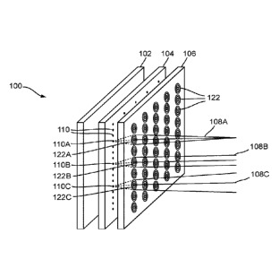
Turning now to FIGs. 3 and 4, a light-emitting apparatus (also denoted
"lighting apparatus"
or "light apparatus") is shown and is generally identified using reference
numeral 100, according
to some embodiments of this disclosure. Herein, the light-emitting apparatus
may be an apparatus
for illumination, an apparatus for facilitating the growth of plants, or an
apparatus for display an
image or a video thereon.
The light-emitting apparatus 100 in these embodiments comprises a light-
emitting
layer 104 sandwiched between a substrate 102 and an optical-transformation
layer 106 for
emitting light 108 from the light-emitting layer 104 through the optical-
transformation layer 106.
When the emitted light 108 goes through the optical-transformation layer 106,
the optical-
transformation layer 106 adjusts one or more parameters of the light 108 such
as the amplitude or
intensity, phase, polarization, pattern, direction, and the like.
The light-emitting layer 104 may be any suitable lighting devices. In these
embodiments,
the light-emitting layer 104 is printed, coated, or otherwise coupled to the
substrate 102 and
comprises a plurality of light-emitting diodes (LEDs) 110 arranged in a matrix
form although
other arrangements of the LEDs 110 are also readily available. Herein, the
LEDs 110 may be any
suitable LEDs such as conventional LEDs, quantum dot (QD) LEDs, organic LEDs
(OLEDs),
and/or the like.
The optical-transformation layer 106 is printed, coated, or otherwise coupled
to the light-
emitting layer 104 for adjusting or otherwise transforming the parameters of
the light emitted from
the light-emitting layer 104 (described in more detail later).
The optical-transformation layer 106 comprises one or more optical-
transformation
units 122 arranged in a predefined pattern with each optical-transformation
unit 122 comprising a
metasurface. Herein, a metasurface is a two-dimensional array of nano-
structures with a
subway elength spacing and may be used for modulating electromagnetic waves.
The detail of
metasurface is described in the academic paper entitled "LIGHT PROPAGATION
WITH PHASE
DISCONTINUITIES: GENERALIZED LAWS OF REFLECTION AND REFRACTION," by
Nanfang Yu, Patrice Genevet, Mikhail A. Kats, Francesco Aieta, Jean-Philippe
Tetienne, Federico
Capasso, and Zeno Gaburro, Science volume 334, issue 6054, pages 333-337
(2011).
As shown in FIGs. 5 and 6, each metasurface unit 122 comprises a metasurface
having a
subwavelength thickness (i.e., the thickness thereof being smaller than the
wavelength of the light
emitted from the light-emitting layer 104) and comprising a plurality of nano-
scale structures 124
arranged in a periodical manner with a specific order for precisely adjusting
or transforming
characteristics or parameters (e.g., amplitude or intensity, phase,
polarization, pattern, direction,
11
CA 03122600 2021-06-09
WO 2020/252585
PCT/CA2020/050849
and the like) of incident light, thereby allowing precise control of the
properties of the light output
therefrom.
In some embodiments, the nano-scale structures 124 (also denoted "nano-
structures") may
be subwavelength structures made of suitable metal or dielectric materials
with one or more
dimensions thereof being smaller than the wavelength of the light emitted from
the light-emitting
layer 104. In some embodiments, the nano-scale structures 124 may comprise a
plurality of
nanorods (also denoted "antennas"; see FIG. 6). In some embodiments, the nano-
scale
structures 124 may comprise a plurality of V-shaped nanorods. As described
above, the nano-
scale structures 124 form a periodic or repetitive pattern and each pattern
may comprise a plurality
of nano-scale structures 124 of different shapes and dimensions.
Depending on the geometry and distributions of the nano-structures 124, the
optical-
transformation layer 106 may be configured for adjusting or transforming one
or more parameters
of the incident light.
For example, as shown in FIG. 4, a metasurface unit 122A of the optical-
transformation
layer 106 may be configured for phase transformation of an incident light 108A
and modifying
the direction thereof to be convergent thereby forming a convergent light beam
focusing at a
desired point spaced from the optical-transformation layer 106.
As another example, a metasurface unit 122B of the optical-transformation
layer 106 may
be configured for phase transformation of an incident light 108B and modifying
the direction
thereof to be collimated thereby forming a collimated light beam for reaching
a target at distance.
As a further example, a metasurface unit 122C of the optical-transformation
layer 106 may
be configured for phase transformation of an incident light 108C and modifying
the direction
thereof to be divergent thereby forming a divergent light beam for
illuminating a large area.
In conventional grow-light applications, one or more lighting devices (also
called grow-
light devices) are used for emitting light towards the plants for facilitating
the growth thereof In
these applications, a portion of the light emitted from the grow-light devices
such as light emitted
from the peripheral area of the grow-light devices may only partly impinge the
plants due to the
divergent nature of the light beams thereby wasting the optical energy. Such
an issue may be more
significant if the plants are spaced from each other.
In some embodiments, the light-emitting apparatus 100 may be used as a grow-
light device
without or at least alleviating the above-mentioned issue. In these
embodiments, the optical-
transformation layer 106 or at least some metasurface units 122 thereof may be
designed to modify
the direction of the incident light 108 towards the plants. For example, the
optical-transformation
layer 106 may be designed to adjust the light emitted from the peripheral area
of the light-emitting
layer 104 towards the plants while making the light emitted from the central
area of the light-
12
CA 03122600 2021-06-09
WO 2020/252585
PCT/CA2020/050849
emitting layer 104 more divergent to cover more areas of the plants, thereby
giving rise to
significantly more efficient illumination.
In some embodiments, the optical-transformation layer 106 or at least some
metasurface
units 122 thereof may be designed to adjust the parameters of the light
emitted from the light-
emitting layer 104 for optimizing the illumination configurations of the
plants and adapting to the
grow-needs thereof
In some embodiments, the optical-transformation layer 106 or at least some
metasurface
units 122 thereof may be designed to adjust the light emitted from the light-
emitting layer 104
towards desired directions to form areas with high or low light-concentrations
thereby creating
hot or cool spots at target illumination areas. Such hot or cool spots may be
created for treating
damaged areas of the plants or for illuminating fragile parts thereof.
FIG. 7 is a schematic exploded view of a light-emitting apparatus 200
according to some
embodiments of this disclosure. In these embodiments, the light-emitting
apparatus 200 is similar
to the light-emitting apparatus 100 in the embodiments shown in FIGs. 3 and 4
except that the
.. light-emitting apparatus 200 further comprises a polarization-control layer
202 sandwiched
between the light-emitting layer 104 and the optical-transformation layer 106.
Moreover, in these embodiments, the optical-transformation layer 106 may be
polarization-selective. In particular, each metasurface unit 122 may be
selective of a specific
polarization, i.e., only allow light with a specific polarization state to
pass therethrough and block
.. light with other polarization states. Different metasurface units 122 of
the optical-transformation
layer 106 may have same or different polarization-selectivity settings,
depending on the
implementation.
The polarization-control layer 202 is made of a suitable material that
polarizes incident
light when the incident light travels therethrough (represented by the
circular arrows 204 and 206
in FIG. 7). In some embodiments, the polarization-control layer 202 may form a
single
polarization-control unit and polarize the incident light to a predefined
polarization state.
In some other embodiments, the polarization-control layer 202 may form a
single
polarization-control unit and comprise liquid crystals with voltage-controlled
retardations.
Therefore, the polarization of the polarization-control layer 202 may be
controlled by adjusting
the voltage applied thereto.
In yet some other embodiments, the polarization-control layer 202 may comprise
a
plurality of polarization-control units (not shown) corresponding to the
plurality of metasurface
units 122 of the optical-transformation layer 106. At least some polarization-
control units may be
made of liquid crystals and the polarization thereof are controllable by
adjusting the voltage
applied thereto.
13
CA 03122600 2021-06-09
WO 2020/252585
PCT/CA2020/050849
The optical-transformation layer 106 thus exhibits a selective response to
light of distinct
polarization states. In some embodiments, the light-emitting apparatus 200 may
be used as a
display which may quickly switch between displaying different images without
the need of
adjusting the light source (e.g., the light-emitting layer 102). The switching-
display or illumination
patterns may be encoded into a polarization pattern of the optical-
transformation layer 106 and/or
the voltage pattern thereof for automatic pattern-switching.
For example, in some embodiments, the light-emitting apparatus 200 may be used
as a
display and the polarization-control layer 202 and the optical-transformation
layer 106 thereof
may each comprise a plurality of units forming corresponding pixels 232 and
234, respectively,
with each pixel comprising one or more subpixels (see FIGs. 8A to 10B).
In one embodiment as shown in FIGs. 8A and 8B, each pixel 232 of the
polarization-
control layer 202 comprises a plurality of subpixels (e.g., two subpixels 242A
and 242B). Thus,
the polarization-control layer 202 comprises a plurality of subpixel sets
(also identified using
reference numeral 242A and 242B) with each set comprise a respective subpixel
242A or 242B
of each pixel 232. Each subpixel set is configured to a specific polarization
setting (see FIG. 8A).
As shown in FIG. 8B, each pixel 234 of the optical-transformation layer 106
has one
metasurface subpixel (also denoted using reference numeral 234) which is
controlled to switch
between two polarization-selectivity and phase-transformation settings
(indicated by the
symbols 246).
During operation, the light-emitting layer 104 emits light (not shown). With
suitable
polarization settings, each subpixel set of the polarization-control layer 202
adjusts the light
emitted from the light-emitting layer 104 and form two light beams (not shown)
with different
polarization states. The two light beams are overlapped and incident into the
optical-
transformation layer 106.
The metasurface subpixels 234 of the optical-transformation layer 106 are
controlled to
switch between two polarization-selectivity and phase-transformation settings
246 with the first
polarization-selectivity setting suitable for allowing the light beam from the
first subpixel set 242A
to pass therethrough and the second polarization-selectivity setting suitable
for allowing the light
beam from the second subpixel set 242B to pass therethrough. Consequently, the
light-emitting
apparatus 200 alternately displays two images 222 and 224 (see FIGs. 11A and
11B) at two
directions. Depending on the phase-transformation settings, the two directions
may be two
different directions as shown in FIGs. 11A and 11B, or may be the same
direction.
The switching of the polarization-selectivity and phase-transformation
settings of the
optical-transformation layer 106 (also denoted as the refresh rate) may be at
a slow rate or
frequency to alternately displays the two images 222 and 224 in a palpable
manner such as
14
CA 03122600 2021-06-09
WO 2020/252585
PCT/CA2020/050849
displaying the first image 222 for a few second at the first location and then
displaying the second
image 224 at the second location for another few seconds (FIGs. 11A and 11B).
Alternatively, the
refresh rate of the optical-transformation laver 106 may be at a high
frequency (e.g., greater than
or equal to 60 frames per second) such that the two images 222 and 224 are
effectively
simultaneously displayed at the two locations to human eyes (see FIG. 12).
In one embodiment as shown in FIGs. 9A and 9B. each pixel 232 of the
polarization-
control layer 202 has one metasurface subpixel (also denoted using reference
numeral 232) which
is controlled to switch between two polarization settings (see FIG. 9A,
indicated by the
symbols 248).
As shown in FIG. 9B, each pixel 234 of the optical-transformation layer 106
comprises a
plurality of subpixels (e.g., two subpixels 244A and 244B). Thus, the optical-
transformation
layer 106 comprises a plurality of subpixel sets (also identified using
reference numeral 244A
and 244B) with each set comprise a respective subpixel 244A or 244B of each
pixel 234. Each
subpixel set is configured to a specific polarization-selectivity and phase-
transformation setting.
During operation, the light-emitting layer 104 emits light (not shown). The
polarization-
control layer 202 adjusts the light emitted from the light-emitting layer 104
and form a light beam
(not shown) with switching polarization states so as to pass through the first
subpixel set 244A of
the optical-transformation layer 106 or pass through the second subpixel set
244B thereof.
Depending on the refresh rate of the optical-transformation layer 106, the
light-emitting
apparatus 200 may alternately display two images 222 and 224 at two locations
in a palpable
manner or effectively simultaneously to human eves (see FIGs. 11A, 11B, and
12).
In one embodiment as shown in FIGs. 10A and 10B, each pixel 232 of the
polarization-
control layer 202 comprises a plurality of subpixels (e.g., two subpixels 242A
and 242B). Thus,
the polarization-control layer 202 comprises a plurality of subpixel sets
(also identified using
reference numeral 242A and 242B) with each set comprise a respective subpixel
242A or 242B
of each pixel 232. Each subpixel set is configured to a specific polarization
setting (see FIG. 10A).
Correspondingly and as shown in FIG. 10B, each pixel 234 of the optical-
transformation
layer 106 comprises a plurality of subpixels (e.g., two subpixels 244A and
244B). Thus, the
optical-transformation layer 106 comprises a plurality of subpixel sets (also
identified using
reference numeral 244A and 244B) with each set comprise a respective subpixel
244A or 244B
of each pixel 234. Each subpixel set is configured to a specific polarization-
selectivity and phase-
transformation setting. The polarization-selectivity setting of each subpixel
set 244A or 244B
matches the polarization setting of each subpixel set 242A or 242B (i.e.,
allowing the light from
the corresponding subpixel 242A or 242B to pass therethrough).
CA 03122600 2021-06-09
WO 2020/252585
PCT/CA2020/050849
During operation, the light-emitting layer 104 emits light (not shown). Each
subpixel
set 242A or 242B of the polarization-control layer 202 adjusts the light
emitted from the light-
emitting layer 104 and form two light beams (not shown) with different
polarization states. The
two light beams are overlapped and incident into the optical-transformation
layer 106. Each light
beam from the polarization-control layer 202 passes through a correspondingly
subpixel set 244A
or 244B of the optical-transformation layer 106, thereby simultaneously
forming two images 222
and 224 at two directions (see FIG. 12).
In some embodiments, the light-emitting apparatus 200 may be used as an
illumination
device which may quickly switch between different illumination patterns.
Moreover, the light-
emitting apparatus 200 may be used as a grow-light device with customized
polarization patterns
adapting to the plants having highly-ordered constituents sensitive to light
polarization. For
example, some plants may absorb or reflect light with a specific polarization
state significantly
more efficient than light with other polarization states. Therefore, the light-
emitting apparatus 200
may be used as a grow-light device with customized polarization patterns
adapting to the plants'
needs for optimizing the photosynthesis process thereof The structure of the
illumination
device 200 in various embodiments may be similar to that shown in FIGs. 8A to
10B.
By using metasurfaces in the optical-transformation layer 106, the lighting
device
disclosed herein may efficiently couple the optical energy into fiber-optic
cables. For example,
FIG. 13 is a schematic exploded view of a light-emitting apparatus 300
according to some
embodiments of this disclosure. In these embodiments, the light-emitting
apparatus 300 is similar
to the light-emitting apparatus 100 in the embodiments shown in FIGs. 3 and 4
and further
comprises a plurality of fiber-optic cables 302 adjacent respective
metasurface units 122. Each
metasurface unit 122 is configured to form a convergent light beam incident
into the
corresponding fiber-optic cable 302. Such a lighting device 300 may be used in
various
applications such as efficient indoor illumination, locally optimized
illumination of plants, and
efficient distribution of optical energy over a target area.
Although in the embodiments shown in FIG. 13, the light-emitting apparatus 300
is similar
to the light-emitting apparatus 100 (i.e., having three layers 102, 104, and
106), in some
embodiments, the light-emitting apparatus 300 may be similar to the light-
emitting apparatus 200
(i.e., having four layers 102, 104, 202, and 106).
In above embodiments, the lighting device 100, 200, or 300 only comprises one
optical-
transformation layer 106. In some embodiments, the lighting device may
comprise a plurality of
optical-transformation layers 106. In some embodiments, at least some of the
plurality of optical-
transformation layers 106 may be polarization-selective, and different optical-
transformation
16
CA 03122600 2021-06-09
WO 2020/252585
PCT/CA2020/050849
layers 106 may have same or different polarization-selectivity settings,
depending on the
implementation.
As described above, various layers of the light-emitting apparatus 100 such as
the optical-
transformation layer 106 may be printed to the substrate 102 or onto each
other using any suitable
printing technology.
For example, FIG. 14 is a conceptual diagram showing the printing of some
layers such as
the optical-transformation layer 106 the light-emitting layer 104 in some
embodiments.
As shown, the substrate 102 (with the light-emitting layer 104 printed or
otherwise coupled
thereon) arranged on a flat surface of a platform 342. A printing device (not
shown) with a slot-
die head 344 is used for printing the sublayers/layers. The slot-die head 344
comprises an ink
cartridge 346 filled with respective "ink" and moves (indicated by the arrow
348) on the substrate
102 (or in particular the printed light-emitting layer 104) to deposit the
metasurface material from
the ink cartridge 346 thereto to form the one or more metasurface optical-
transformation units 122.
Herein, the "ink" refers to sublayer/layer material in a suitable form such as
a solution, a
gel, or powder that is used as a precursor for the fabrication of layers.
During the slot-die
fabrication of each layer, heat treatment is usually used for evaporating the
solvent or for melting
the powders to solidify the fabricated layer.
FIG. 15 is a schematic diagram of a lighting system 400 for facilitating the
growth of one
or more plants 410 according to some embodiments of this disclosure. As shown,
the system 400
comprises a power source 402 powering a control circuitry 404 and a light-
emitting apparatus 406
which may be any of the above-described light-emitting apparatus 100, 200, or
300. The control
circuitry 404 controls the light-emitting apparatus 406 for emitting light 408
with customized
parameters for illuminating the plants 410 to facilitate the growth thereof.
FIG. 16 is a schematic diagram of a lighting system 500 for facilitating the
growth of plants
according to some embodiments of this disclosure. The lighting system 500 in
these embodiments
is similar to the lighting system 400 shown in FIG. 14 and further comprises a
sensor 412 for
monitoring the growth of the plants 410, such as a light sensor for monitoring
the light 414
reflected from the plants 410, and provides feedback to the control circuitry
404 for adjusting the
light parameters as described above to optimize the illumination configuration
to better facilitate
the growth of the plants 410.
In some embodiments, the light-emitting layer 104 may be transparent LED layer
and the
light-emitting apparatus 100, 200, or 300 may further comprise a solar-cells
layer "behind- the
light-emitting layer 104 (i.e., between the substrate 102 and the light-
emitting layer 104) haying
one or more photovoltaic cells (also denoted "solar cells") for converting
light energy to electrical
energy, and an electronic-power converter layer behind the solar-cells layer.
The detail of the
17
CA 03122600 2021-06-09
A8142819W0
solar-cells layer and the electronic-power converter layer is described in
Applicant's copending
US provisional patent application Ser. No. 62/831,828, entitled "HYBRID-ENERGY
APPARATUS, SYSTEM, AND METHOD THEREFOR".
For example, FIG. 17 shows an example of the solar-cells layer 540 comprising
a plurality
of sublayers. As shown, the solar-cells layer 500 in this example comprises an
anode sublayer 542
made of suitable material such as Indium Tin Oxide (ITO), a sublayer of Zinc
Oxide (ZnO) 544,
a sublayer of poly(ethylenimine) and poly(ethylenimine) ethoxylated (i.e.,
PEIE) 546, a sublayer
of organic solar-cells 548 such as a sublayer of polymer solar-cells such as a
sublayer of bulk
heterojunctions (BHJs), a sublayer of Molybdenum trioxide (Mo03) 550, and a
cathode
sublayer 552 made of suitable material such as silver (Ag) or Aluminum (Al).
The anode 542 and
the cathode 552 are electrically connected to other layers such as the
electronic-power
converter layer.
Lighting System with Controlled Illumination Patterns
FIG. 18 shows a light-emitting apparatus 600 in some embodiments for use as an
illumination or light source with controlled illumination patterns by precise
control of light
deflection angles using metasurfaces or other light control structures. The
illumination from the
lighting system 600 is distributed according a specific pattern onto the image
plane 612 where one
or more objects such as one or more plants are located therein.
For ease of annotation, the axes x and y denote the orthogonal axes defining
the image
plane 612, the z-axis is an axis along the controllable lighting structure 100
and the image
plane 612 and is orthogonal to the axes x and y (i.e., orthogonal to the image
plane 612), the y-
deflection angle 0 is the angle between the y-axis and the projection of a
light beam 610 on the
image plane 612, and the z-deflection angle co is the angle between the z-axis
and the projection
of the light beam 610 on the x-z plane.
The light-emitting apparatus 600 is similar to the light-emitting apparatus
100 shown in
FIG. 4 and comprises a light-emitting layer 104 having one or more LEDs (not
shown) and an
optical-transformation layer 106 such as a topocentric vector control panel
(TVCP) layer in these
embodiments, in front of the light-emitting layer 104. Although not shown in
FIG. 18, the light-
emitting apparatus 600 may also comprise a substrate 102 for supporting the
light-emitting
layer 104 (similar to the light-emitting apparatus 100 shown in FIG. 4).
The light-emitting layer 104 comprises an array of LEDs as the light source
and emits a
plurality of light beams 610 passing through the TVCP 106 towards the image
plane 612.
18
Date Recue/Date Received 2021-06-09
CA 03122600 2021-06-09
WO 2020/252585
PCT/CA2020/050849
The TVCP 106 comprises one or more optical-transformation units 122 (also
denoted
"lenses" in these embodiments: not shown in FIG. 18) arranged in a predefined
pattern with each
optical-transforntation unit 122 comprising a metasurface. Each optical-
transformation unit 122
of the TVCP 106 controls the direction of a light beam 610 passing
therethrough by controlling
the deflection angles 0 and qt thereof to adjust the azimuth, elevation, and
angle of the cone of
light 610 in the image plane 612.
The TVCP 106 effectively breaks the symmetry of the light distribution
otherwise present
on the image plane 612 (see FIG. 2). Moreover, a small change in the
deflection angles 0 and 9
would give rise to significant change in the light-intensity distribution on
the image plane 612.
Thus, with a carefully configured TVCP 106, the lighting system 600 may use a
plurality of light
beams emitting from the light-emitting layer 104 through the TVCP 106 towards
a plurality of
predefined incidence points distributed on the image plane 612 to generate
almost any light-
intensity distribution in a target illumination area thereon as needed.
The illumination pattern (e.g., the size and shape of the target illumination
area and the
light-intensity distribution therein) and the number of light sources (e.g.,
LEDs) determine the
locations of the predefined incidence points which may be calculated by using
a suitable
optimization method to optimize a suitable cost function with the constraint
that all incidence
points must be within the target illumination area.
For example, to obtain a uniformly distributed (or more precisely, nearly
uniformly
distributed) light-intensity distribution, a Normalized Mean Square Error
(NMSE) of the light-
intensity distribution
NiZliv=1(/ (xi) ¨12)2
NMSE¨ _______________________________________________________ (1)
E7-1 1(x;)
may be used as the cost function where 1.4. is the mean value of the light
intensity on the image
plane 612, I (x i) is the light intensity of the i-th pixel, and Nis the total
number of pixels of the
target illumination area on the image plane 612. A suitable optimization
method may be used to
calculate the deflection angles 8 and yo of each light beam 610 (which
determine the location of
the incidence point thereof) that minimize the NMSE under the constraint that
all incidence points
must be within the target illumination area.
FIG. 19 illustrates the formation of the cost function in one example wherein
a uniform
illumination pattern within a circular target illumination area 622 on the
image plane 612 is to be
generated. Those skilled in the art will appreciate that the cost function for
other illumination
pattern may be similarly formed.
19
CA 03122600 2021-06-09
WO 2020/252585
PCT/CA2020/050849
In the example shown in FIG. 19, the lighting system 600 may use eight (8)
light beams
emitting towards respective incidence points 624 distributed on two concentric
circles 626A
and 626B (four points on each circle) within the circular area 622 of the
image plane 612 with
uniform angular spacing.
Any suitable optimization methods such as an artificial intelligent (AI)
algorithm, a
machine learning algorithm, a gradient descent (GD) method, a simulated
annealing (SA), and/or
the like may be used for finding the global (or near-global) minimum of the
NMSE of Equation
(1) and the corresponding deflection angles 0 and co of each light beam 610.
FIG. 20 is a flowchart showing the steps of a process 640 for finding the
global (or near-
global) minimum of the NMSE of Equation (1) using a GD method which uses the
following
predefined parameters in the optimization:
= Number of LEDs in the light-emitting layer 104;
= Direction and angular span of the field of view (F0V) of each LED:
= The shape of the target illumination area on the image plane 612
= The size of the target illumination area;
= Distance between the source and the target illumination area;
= Learning rate of GD; and
= Maximum number of iterations.
Those skilled in the art will appreciate that the above-described parameters
may be
customized by the user or determined by the setup of the system 600 before the
process 640 starts.
As shown in FIG. 20, after the process 640 starts (step 642), the above-
described
parameters are loaded (step 644) and an initial state (e.g., an initial set of
values for the state
variables (0, co)) of each light beam 610 is randomly selected (step 646).
At step 648, the gradient of the cost function at the current state with
respect to the state
variables (0, 9) of all light beams 610 is calculated. Then, the state
variables (0, 9) of all light
beams 610 are "moved" (i.e., changing the values of the state variables (0,
co)) in the opposite
direction of the gradient value of the current state multiplied by the
learning rate (step 650).
At step 652, the process 640 checks if the number of iterations has reached
the maximum
number of iterations (predefined by the system or by a user). If the number of
iterations has
reached the maximum number of iterations, the optimization has completed and
the process 640
then ends (step 654).
If at step 652, the number of iterations has not reached the maximum number of
iterations,
the process 640 goes to step 656 to check if the incidence point of any light
beam 610 is out of the
target illumination area. If not, the process 640 goes back to step 648 to
further "move- the state
variables (0, co) of the light beams 610.
CA 03122600 2021-06-09
WO 2020/252585
PCT/CA2020/050849
If at step 656, it is determined that the incidence points of one or more
light beams 610 are
out of the target illumination area, then the process 640 recalculates the
values of the state
variables (0, co) of the one or more light beams 610 to locate the incidence
points thereof at the
border of the target illumination area along the opposite direction of the
gradient value, and
defines the one or more light beams as fixed beams (i.e., the state variables
(0, (p) thereof would
no longer be used for optimization) (step 658). Then, the process 640 randomly
selects an initial
state (e.g., an initial set of values for the state variables (0, co)) of each
of the remaining light
beams 610 (step 660), and goes back to step 648 for further optimization.
The process 640 may loop through the above-described steps one or more times
and,
according to the maximum number of iterations, eventually stops the trials and
the global (or near-
global) minimum of NMSE is achieved. The corresponding values of the state
variables (0, 0) of
each light beam 610 are then used for configuring the optical-transformation
units 122 of the
TVCP 106.
In some embodiments, the optimization process may partition the light beams to
a plurality
of groups. For example, in the example shown in FIG. 19, the optimization
process may partition
the light beams to two groups each comprising four light beams whose incidence
points are in a
circle 626A or 626B. Then, the optimization process may form a cost function
wherein the control
variables to minimize the NMSE are the radius and degree of rotation of the
circles 626A
and 626B.
FIGs. 21 to 25 show the optimization results using the GD method for creating
uniform
light-intensity distribution within target illumination areas of different
shapes on the image plane
including a triangular illumination-area (FIG. 21), a square illumination-area
(FIG. 22), a
pentagonal illumination-area (FIG. 23), a circular illumination-area (FIG.
24), and a donut-shape
or ring-shape illumination-area (FIG. 25).
Fabrication Techniques of Metasurfaces
The metasurface-based TVCP 106 may be fabricated using any suitable methods
such as
electron beam lithography. However, this technique is costly and slow
rendering it suitable only
for the fabrication of small metasurfaces. The TVCP 106 described above
usually requires
metasurfaces with diameters in centimeter scales and thus the conventional
electron beam
lithography technique may not be rapid and cost-effective.
In some embodiments, a deep ultraviolet (UV) lithography technique is used for
fabricating metasurfaces such as metasurface-based TVCP 106 described above.
While the deep
UV lithography technique is a well-established technique used in the
semiconductor area, to
Applicant's knowledge, it has not been used in fabricating metasurfaces.
21
CA 03122600 2021-06-09
WO 2020/252585
PCT/CA2020/050849
With this technique, a layer of chromium is deposited on a glass wafer. Then,
the wafer is
spin-coated with a resist followed by UV exposure and developing. Finally, the
metasurface
patterns are defined by etching the chromium layer. Such a technique allows
fabrication of a
plurality of metasurfaces on a large wafer via a single process thereby giving
rise to a rapid and
cost-effective fabrication. Moreover, the deep UV lithography technique also
enables fabrication
of metasurfaces for the visible and infrared wavelength ranges using silica,
titanium dioxide, or
amorphous silicon.
Lighting System with a Uniform Illumination Pattern
As described above, conventional illumination systems such as LED panels used
for
indoor plant growth usually do not produce a uniform distribution of light
over the plants.
In some embodiments similar to those shown in FIGs. 4 and 18, uniform or near-
uniform
illumination of a lighting system 700 such as a grow light system may be
obtained by overlaying
an angle-control optical-transformation layer 106 such as a TVCP layer in
front of the light-
emitting layer 104. As shown in FIG. 26, the light-emitting layer 104 emits a
plurality of light
beams 702 passing through the TVCP 106 towards an image plane (not shown). The
spatial
distribution of each light beam 702 may be characterized by the angles fl, 0,
and 9, wherein the
angle fi determines the angular span of the light beam 702, and the angles 0
and 9 determine the
direction of the light beam 702.
The TVCP 106 comprises one or more optical-transformation units 122 arranged
in a
predefined pattern with each optical-transformation unit 122 comprising a
metasurface. Each
optical-transformation unit 122 of the TVCP 106 is configured for precisely
controlling the angles
fl, 0, and yo of the corresponding light beam 702 to arbitrarily change the
angular extent, altitude,
and latitude of the cone of light in the image plane. The TVCP 106 effectively
breaks the symmetry
of the light distribution otherwise present in the image plane (e.g., see FIG.
2). The use of the
TVCP 106 is powerful in that a small change in the angles fi, 0, and/or 9 may
make significant
difference in the intensity distribution in the image plane. Thus, almost any
arbitrary intensity
distribution may be generated.
The lighting system 700 may be used for generating a uniform illumination
pattern at the
image plane and may be used as a grow light. It is noted that, for ease of
fabrication and
implementation, the number of metasurfaces with different designs needs to be
minimized.
In some embodiments, the TVCP 106 of a uniform-illumination lighting system
700 may
only comprise two types of metasurfaces including a set of splitting
metasurfaces, and a set of
converging metasurfaces.
22
CA 03122600 2021-06-09
WO 2020/252585
PCT/CA2020/050849
The splitting metasurfaces are polarization-sensitive metasurfaces which
modify angles fi,
9, yo of light beams by directing light of two orthogonal polarization states
in opposite directions.
In these embodiments, the light-emitting layer 104 (e.g., LED light-emitting
layer) emits
unpolarized light which ensures equal power split into two opposite directions
at the splitting
metasurfaces.
As shown in FIG. 27A, the splitting metasurfaces 122A and 122B of a TVCP 106
are
configured for distributing light beams 702A and 702B, respectively, at the
borders of intended
illumination pattern on the image plane (not shown).
FIG. 27B shows the illumination pattern 704A on the image plane with optical
energy
significantly distributed along vertical borders (the directed lights are
denoted -vertical-border-
focused lights" hereinafter), created by using splitting metasurfaces to split
the light from the light-
emitting layer to vertically direct light to the corresponding borders.
Similarly, FIG. 27C shows the illumination pattern 704B on the image plane
with optical
energy significantly distributed along horizontal borders (the directed lights
are denoted
"horizontal border-focused lights- hereinafter), created using 90 -rotated
splitting metasurfaces
(similar to the splitting metasurfaces used in FIG. 27B but with 90 rotation
of the optical energy
distribution) to split the light from the light-emitting layer to horizontally
direct light to the
corresponding borders.
The horizontal/vertical border-focused lights as shown in FIG. 27B may be
directed to a
same target area on the image plane to allow the lights directed therefrom to
overlap and form an
illumination pattern 706 with optical energy substantially concentrated along
the four borders of
the area; see the conceptual representation in FIG. 28.
As shown in FIGs. 29A and 29B, converging metasurfaces 122C are configured for
modifying angle /I of the light beam 702C without any change in the direction
of the cone of light
beam 702C. Thus the converging metasurfaces 122C distribute light beams 702C
at the center of
a target area on the image plane thereby creating an illumination pattern with
optical energy
substantially focused at the center thereof
As illustrated by the conceptual representation shown in FIG. 30, by using the
splitting
metasurfaces 122A and 122B and the converging metasurfaces 122C to direct
light beams to a
same target area, the illumination patterns 706 (which is a combination of
illumination
patterns 704A and 704B shown in FIG. 28) and 708 may be combined to obtain a
uniform light
distribution in the target area.
Such a uniform light distribution is substantially independent of the distance
between the
metasurface-based TVCP 106 and the image plane 712. As shown in FIG. 31, the
light distribution
is merely scaled at different distances without compromising the uniformity of
distribution.
23
CA 03122600 2021-06-09
WO 2020/252585
PCT/CA2020/050849
FIG. 32 shows an example implementation of the TVCP 106 using an array of
metasurfaces 122. For ease of illustration, only two metasurfaces 122 are
shown.
In these embodiments, the TVCP 106 comprises a metasurface housing 722
overlaying the
LEDs 110 mounted on a printed circuit board (PCB) 724 of the light-emitting
layer 104. The
metasurface housing 722 comprises a plurality of receptacles 726 at locations
corresponding to
the LEDs 110. Each receptacle 726 comprises with an outwardly expanding inner
surface having
an inner opening for receiving light emitted from the light-emitting layer 104
and an outer opening
for passing through the received light, the outer opening having an area
greater than that of the
inner opening.
In these embodiments, the inner surface of the receptacle 726 is reflective
for reflecting
light rays (emitted from the LED 110 therein) with high angles to contribute
to the overall
illumination, thereby increasing the efficiency of overall lighting. The
maximal light throughput
is accomplished when the cross-section of the inner surface is in a paraboloid
shape and the LED
is located at the foci thereof FIG. 33 is a photo showing the metasurface
housing 722 coupled to
the light-emitting layer 104.
A plurality of metasurface units 122 are fixed or otherwise coupled to the
receptacles 726
of the metasurface housing 722 using suitable fastening means such as epoxy,
glue, and/or the
like, thereby ensuring the alignment of LEDs 110 and metasurface units 122.
Polarization-Selective Illumination
Plants are often composed of constituents with organized arrangements. As a
result, plants'
light absorption is often polarization-sensitive. In other words, plants may
absorb more light in
one particular polarization state than light in the other polarization state.
Therefore, photosynthesis
may be optimized using illumination with specific polarization state.
In some embodiments, the metasurface-based optical-transformation layer 106 of
the grow
light disclosed herein may be polarization-selective, which may be implemented
by arranging the
nano-scale structures 124 of the metasurface to have an asymmetric base
geometry 732 as shown
in FIG. 34. Thus, a grow light with such a metasurface-based optical-
transformation layer 106
may be used for illuminating plants with light of specific polarization state
to optimize light for
photosynthesis. Generally, the metasurfaces of the optical-transformation
layer 106 may be
designed to illuminate plants with a variety of polarization states including
linear, circular, and in
general elliptic polarizations states. Linear polarization illumination may be
used for optimizing
photosynthesis of plants made of fibers oriented in a specific direction, and
circular polarization
illumination may be used for optimizing photosynthesis of plants made of
constituents with
helicity.
24
CA 03122600 2021-06-09
WO 2020/252585
PCT/CA2020/050849
Metasurface-Based TVCP for Photovoltaic Cells
In solar batteries, while always desirable, a perfect light absorption by the
photovoltaic
cells thereof is difficult to achieve due to a mismatch between the spectrum
of the incident light
and the spectral response of the photovoltaic cells. As shown in FIG. 35,
light reflections 842
occurred at the surface of the photovoltaic cells 844 also causes loss of
solar energy that may
otherwise be absorbed by the photovoltaic cells 844.
In some embodiments, the metasurface-based TVCP may be incorporated in
photovoltaic
panels having, e.g., one or more silicon-based and/or one or more quantum-dot
photovoltaic cells,
in which the metasurface-based TVCP may be configured to efficiently deliver
light of specific
wavelengths to the photovoltaic cells. Moreover, the metasurface-based TVCP
allows significant
size-reduction of photovoltaic panels.
As those skilled in the art will appreciate, metasurfaces comprise nanoscale
structures. The
geometry and distribution of the nanoscale structures thereof may be designed
or otherwise
configured for meeting the requirements of a specific application. For
example, metasurfaces may
be designed to pass or otherwise transmit therethrough a portion of the
incident light of a target
spectrum and completely reflect the other portion of the incident light out of
the target spectrum.
In some embodiments as shown in FIG. 36, the metasurface-based TVCP 106 may be
arranged in front of a photovoltaic panel 852 having, e.g., one or more
silicon-based and/or
quantum-dot photovoltaic cells. The metasurface-based TVCP 106 comprises a
plurality of
metasurface units (not shown) having a spectral response matching that of the
photovoltaic cells.
Thus, the combination of the metasurface-based TVCP 106 and the photovoltaic
panel 852 is
significantly more efficient compared to the photovoltaic panel 852 alone
because, when the
photovoltaic panel 852 is used alone, the spectrum that are not fully absorbed
may turn into heat
and other unwanted effects that degrade the performance thereof Such an
arrangement or
combination is particularly important for indoor photovoltaic cells that
harvest optical energy from
an artificial lighting source such as LEDs wherein the metasurface units may
be designed to match
a specific illumination spectrum of the light source and reject other light
that cannot be efficiently
absorbed by the photovoltaic cells.
Another important application of metasurfaces lies in their above-described
ability to
redirect a light ray to a different direction. As shown in FIG. 37, a
metasurface-based TVCP 106
in front of may be a photovoltaic panel 852 wherein the metasurface-based TVCP
106 is
configured to converge the incoming light rays 854 into a small area of the
photovoltaic panel 852
and thus, the size of the photovoltaic panel 852 may be significantly reduced.
FIG. 38 shows a
prior-art photovoltaic panel 844 without the metasurface-based TVCP 106 for
comparison.
CA 03122600 2021-06-09
WO 2020/252585
PCT/CA2020/050849
Ultra-Directional Screens Using Metasurfaces
Conventional screens or displays usually have wide angular spans of their
fields of view
(F0Vs). However, in some applications, it may be desired to limit the FOV of a
display.
Herein, the term FOV refers to the angular extent of illumination (e.g., in a
cone shape or
other shape) emitted from a component (e.g., a LED layer, a metasurface layer,
or the like),
wherein in various embodiments, the light may be used for illumination or for
displaying one or
more images. The FOV may be characterized by the direction and three-
dimensional (3D) angular
span of the light emitted from the component.
For example, a display in a vehicle or an airplane is generally watched only
by an
individual. However, as shown in FIG. 39, a display 862 with a wide FOV 868
(i.e., the FOV 868
having a wide angular span) in a vehicle or an airplane (not shown) would
unnecessarily emit light
to surrounding areas which may result in lowered brightness to the user 864 in
front thereof, waste
of optical energy, and disturbance to people 866 adjacent thereto.
Similarly, a wide-FOV display used in homes or theatres would light up
peripheral areas
such as walls and ceiling, leading to lowered brightness to the users in front
thereof and waste of
optical energy.
Moreover, in some applications requiring enhanced security or privacy such as
displays of
ATMs, displays in banks, laptop displays with which users are using for
sensitive work, may
require highly directional displays, as wide-FOV displays in these
applications may also cause
security or privacy risks in addition to above-described issues of lowered
brightness, waste of
optical energy, and/or disturbance to people adjacent thereto.
FIG. 40 shows an ultra-directional screen or display 870 using metasurfaces,
according to
some embodiments of this disclosure. The ultra-directional screen 870
comprises a display or
display layer 872 and a metasurface panel or layer 874 in front thereof
Similar to the optical-transformation layer 106 described before, the
metasurface
panel 874 comprises a plurality of metasurface units constructed in an array
of nanoscale
structures that direct light to desired directions so as to restrict the light
emitted from the
display 872 within a predefined FOV 878 smaller than the FOV 876 of the
display 872, thereby
creating a virtual visual-barrier so that only the intended person 864 can see
the content shown on
the display 872.
This ultra-directional screen 870 has a number of advantages including:
= superior brightness due to the concentrated distribution of light energy
into a
smaller area;
26
CA 03122600 2021-06-09
WO 2020/252585
PCT/CA2020/050849
= improved power-efficiency due to the avoidance of illuminating unintended
areas
and uniform distribution of light energy onto the intended area; and
= enhanced security and privacy as visual information can only be viewed by
the
intended person in front thereof
As described above, metasurfaces may be designed to interact differently with
light of
different polarization states, which is accomplished by fabricating the
nanostructures of the
metasurfaces with an asymmetric geometry.
FIG. 41 shows a variable-fields-of-view (VFOV) screen or display 880 in some
embodiments. The MFOV display 880 comprises a display 872, a polarization
control panel 884
in front of the display 872, and a polarization-sensitive metasurface panel
886 in front of the
polarization control panel 884.
In these embodiments, the polarization control panel 884 may be implemented
using liquid
crystal polarization rotators and is controlled by an adjustable control
signal V for controlling the
polarization of the light emitted from the display 872 to either one of the
two orthogonal
polarization states.
While the MFOV display 880 is similar to the light-emitting apparatus or
display 200
shown in FIGs. 11A, and 11B, the MFOV display 880 in these embodiments does
not direct lights
with different polarization states to FOVs of different directions as the
light-emitting apparatus or
display 200 shown in FIGs. 11A, and 11B does. Rather, the polarization-
sensitive metasurface
panel 886 in these embodiments interacts with the polarized light for
directing the light in a first
polarization state to a first FOV with a first angular span 888 and directing
the light in a second
polarization state to form a second FOV with a second angular span 890. For
example, the first
angular span 888 may be a wide angular span suitable for multiple users 864
and 866 about the
MFOV display 880 to view the displayed content, and the second angular span
890 may a narrow
angular span smaller than the firs angular span 888 for only allowing the user
864 to view the
displayed content.
In above embodiment, the polarization control panel 884 polarizes all light
passing
therethrough into the first polarization state when the control signal is at a
first voltage, and
polarizes all light passing therethrough into the second polarization state
when the control signal
is at a second voltage. In this way, the user 864 may switch the FOV of the
MFOV display 880
between the first and second angular spans for sharing the displayed content
to people adjacent
thereto and for creating a virtual visual barrier to prevent other people from
viewing the displayed
content, respectively.
27
CA 03122600 2021-06-09
WO 2020/252585
PCT/CA2020/050849
In another embodiment shown in FIG. 42, the MFOV display 880 is similar to the
display
described in FIGs. 10A and 10B. Specifically, the display 872 comprises two
sets units (pixels or
subpixels, depending on the design) wherein each set of units may be used for
displaying an image.
Correspondingly, each of the polarization control panel 884 and the
polarization-sensitive
metasurface panel 886 also comprises two sets units corresponding to the two
sets of units of the
display 872. Each set of units of the polarization control panel 884 is
controlled by a separate
control signal V1 or V2, and each set of units of the polarization-sensitive
metasurface panel 886
matches a specific polarization state and directs the light with the
polarization state to a specific
FOV.
Therefore, the display 872 may use the two sets of pixels/units to
simultaneously display
two images and polarization control panel 884 polarizes the lights of the
first and second images
into a first and a second polarization states. Then, the polarization-
sensitive metasurface panel 886
directs the light in the first polarization state (i.e., the first image) to a
first FOV with a wide
angular span for sharing the first image with multiple people 864 and 866 and
the light in the
second polarization state (i.e., the second image) to a second FOV with a
narrow angular span for
preventing people 866 from viewing the second image.
For example, as shown in FIGs. 43A and 43B, the display is to simultaneously
display two
images 892A and 892B with the image 892A to be displayed in a first FOV of a
wide angular span
and the image 892B to be displayed in a second FOV of a narrow angular span.
As shown in FIG. 43C, the display 872 partitions the pixels into a first set
of pixels 894A
and a second set of pixels 894B arranged side-by-side for displaying the
images 892A and 892B
simultaneously and side-by-side.
As shown in FIG. 43D, the polarization control panel 884 comprises a plurality
of
polarization units 894 corresponding to the pixels of the display 872 with a
first set of polarization
units 896A corresponding to the first set of pixels 894A for polarizing lights
passing therethrough
to a first polarization state and a second set of polarization units 896B
corresponding to the second
set of pixels 894B for polarizing lights passing therethrough to a second
polarization state.
As shown in FIG. 43E, the polarization-sensitive metasurface panel 886
comprises a
plurality of metasurface units 898 corresponding to the polarization units 894
of the polarization
control panel 884 and directing lights passing therethrough in the first
polarization state to the first
FOV (having a wide angular span) and directing lights passing therethrough in
the second
polarization state to the second FOV (having a narrow angular span).
As a result, the first image 892A is directed to the first FOV and the second
image 892B
is directed to the second FOV. As shown in FIG. 43F, the images 892A and 892B
are visible to
the user 864 located in both the first and second FOVs, and the users 866
located only in the first
28
CA 03122600 2021-06-09
WO 2020/252585
PCT/CA2020/050849
FOV (with wide angular span) can only see the first image 892A In other words,
the image 892B
is invisible to the users 866 located only in the first FOV.
Three-Dimensional (3D) Display Using Metasurfaces
FIG. 44 shows a 3D display 900 using metasurfaces, according to some
embodiments of
this disclosure. As shown, the 3D display 900 comprises a display 872 and a
polarization-sensitive
metasurface panel 886 in front thereof. The display 872 displays an image by
emitting unpolarized
light (which generally comprises both polarization states). The polarization-
sensitive metasurface
panel 886 is configured to direct the light in the first polarization state
into a first FOV 888 and
the light in the second polarization state into a second FOV 890 laterally
slightly offset from the
first FOV 888. A user 864 wearing a pair of glasses with lenses polarized to
different polarization
states then sees a first image in one eye and a second image in the other eye
wherein the second
image is of slight perspective distortion from the first image, thereby
creating a 3D perception of
the displayed image.
In some embodiments, the 3D display 900 may also comprise a polarization
control
panel 884 sandwiched between the display 872 and the polarization-sensitive
metasurface
panel 886. The polarization control panel 884 alternately polarizes the light
from the display 872
to the first and second polarization states in operation.
FIG. 45 shows a 3D display 920 using metasurfaces, according to some
embodiments of
this disclosure. The 3D display 920 is similar to that shown in FIG. 44.
However, the polarization-
sensitive metasurface panel 886 is configured to direct the light in the first
polarization state into
a first FOV 888 that only covers a first eye of the user 864 and the light in
the second polarization
state into a second FOV 890 hat only covers a second eye of the user 864.
Therefore, the user 864,
without wearing a pair of glasses with polarized lenses, may see a first image
in one eye and a
second image in the other eye wherein the second image is of slight
perspective distortion from
the first image, thereby creating a 3D perception of the displayed image.
In some embodiments, the 3D display 920 may also comprise a polarization
control
panel 884 sandwiched between the display 872 and the polarization-sensitive
metasurface
panel 886. The polarization control panel 884 alternately polarizes the light
from the display 872
to the first and second polarization states in operation.
Solar-Cell Angle Correction
In prior art, a solar panel may experience a sunlight reflection issue.
As those skilled in the art understand, the sunlight incident angle may have
significant
impact to the efficiency of photovoltaic cells. As shown in FIG. 46, the
photovoltaic cells of a
29
CA 03122600 2021-06-09
WO 2020/252585
PCT/CA2020/050849
solar panel 942 are of the highest efficiency when the sunlight 944 impinges
the photovoltaic cells
perpendicularly.
As shown in FIG. 47, at a different time when the sunlight 944 becomes at a
non-
perpendicular angle to the photovoltaic cells of the solar panel 942, a
portion 946 of the sunlight
is reflected and the efficiency of the photovoltaic cells is reduced. Thus,
the photovoltaic cells of
a fixed solar panel would have different efficiency at different times of a
day and at different days
of a year. While sun tracking systems have been used for improving the
efficiency of photovoltaic
panels by rotating the solar panel to follow the sun, such systems require
tracking systems and
moving parts, rendering them expensive in manufacturing and use.
FIGs. 48 and 49 show a solar-energy harvesting apparatus 970 which comprises a
solar
panel 972 having one or more photovoltaic cells and a plurality of TVCPs 974
in front thereof
By using polarization sensitive metasurfaces where the response of each TVCP
974 may vary
using an embedded polarization control panel, the plurality of TVCPs 974 may
change the
direction of sunlight 944 such that the incident sunlight 944 at an incident
angle within a
predefined range becomes perpendicular to the photovoltaic cells when
impinging the solar
panel 972, thereby improving the efficiency without the need of a sun-tracking
system or
moving parts.
In some embodiments described above, the light-emitting apparatus and/or
system is used
for plant growth such as for indoor or outdoor plant growth. However, those
skilled in the art will
appreciate that the light-emitting apparatus and/or system disclosed herein
may be alternatively
used in other applications such as street lights.
Although embodiments have been described above with reference to the
accompanying
drawings, those of skill in the art will appreciate that variations and
modifications may be made
without departing from the scope thereof as defined by the appended claims.