Note: Descriptions are shown in the official language in which they were submitted.
A8140854W0
MULTIPLE-LAYER QUANTUM-DOT LED AND METHOD OF FABRICATING
SAME
FIELD OF THE DISCLOSURE
The present disclosure relates generally to a quantum-dot light-emitting
diode, and
in particular to a light-emitting diode having an active emission region with
high external
quantum efficiency formed by a plurality of interleaved quantum-dot layers and
quantum-
barrier layers, and a method of fabricating same.
BACKGROUND
Quantum dots (QDs), a type of semiconductor nanoparticles, have been the
subject
of recent scientific studies. QDs are extremely small nanocrystal
semiconductor materials
with typical diameters of about 2 to 10 nanometers (nm). Compared to bulk
materials, QDs
have many unique characteristics such as high color saturation, narrow
spectra, tunable
emission wavelengths, durability, and simple fabrication process (see
references [1] to [101)
thereby rendering QDs a promising material for making light-emitting diodes
(LEDs)
suitable for various applications such as display devices, lasers, digital
signage,
illumination or lighting devices, and the like. Quantum-dot LEDs (QLEDs) can
have better
energy efficiency due to their high quantum yield for electroluminescence and
their device
structure designed for efficient charge injection. QLEDs usually have much
longer lifetime
comparing to other types of illumination devices such as incandescent
lightbulbs,
fluorescent lightbulbs, and organic LEDs (OLEDs). Moreover, the cost of QLEDs
is also
reduced while mass production thereof becoming available.
QDs exploit the quantum confinement effects in semiconductors. Quantum
confinement effects occur when the size of a particle is at the scale of
electron-hole
distance of an electron-hole pair, also known as the exciton Bohr radius. In
QDs, the sizes
of the crystals are in the same order as the exciton Bohr radius. Such small
sizes imply that
1
Date Recue/Date Received 2020-05-11
CA 03074241 2020-01-28
WO 2019/071362
PCT/CA2018/051297
the crystals are in discrete energy levels which can be explained by the
energy of a particle
in an infinite potential well (also known as a -particle-in-a-box" state). The
relationship of
the energy level of a QD and the size thereof may be described in Equation (1)
which is
the band gap energy for a spherical box (same lengths in all three
dimensions).
p2 X h2
________________________________ = hv, (1)
Ep = 8 x m x L2
where p = 1, 2, ... is the energy level index, Ep is the energy at the p-th
level, h is the
Plank's constant, m is the effective mass of a point charge, and L is the
radius of the particle.
Equation (1) shows that the energy Ep changes with size variation of the QDs
(i.e.,
variation of L) because the excitation in the QDs behaves like a "particle-in-
a-box".
Moreover, Equation (1) indicates that the energy of a particle of light, i.e.,
a photon, is
proportional to its frequency v with the coefficient of the Plank's constant
factor h.
Therefore, changing the size of QDs can create different wavelengths and in
turn different
colors.
Emission spectra of QD solutions show a full width at half maximum (FWHM) of
30 nm to 40 nm, depending on the degree of monodispersity achieved during the
colloidal
synthesis of QD. Smaller FWHM gives rise to higher color purity which is
important in
luminescent applications. Moreover, QDs can be used for white lighting which
can be
evaluated by its color temperature and color rendering index (CR1).
Core-shell type composite quantum dots exhibit properties attractive for light
emitters. It has been shown that over-coating nanocrystallites with higher
band-gap
inorganic materials improves the photoluminescence quantum yields by
passivating non-
radiative recombination sites. Cadmium Selenide/Zinc Sulfide (CdSe/ZnS)
quantum-dot
structure shows high quantum yield (40% to 60%) which makes it a good
candidate as
emitters in QLEDs. In addition to high quantum yield, core-shell CdSe/ZnS
particles have
narrow band edge luminescence, resulting in spanning most of the visible
spectrum (from
470 to 625 nm). ZnS over-coated particles are more robust than organically
passivated dots
and potentially more useful for optoelectronic device structures.
Electroluminescent
devices such as QLEDs can incorporate CdSe/ZnS dots into light-emitting
devices. This
may show greater stability during the fabrication process.
2
CA 03074241 2020-01-28
WO 2019/071362
PCT/CA2018/051297
In addition, CdSe/ZnS have much longer lifetime comparing to bare CdSe quantum
dots due to the surface passivation. In summary, CdSe/ZnS have better energy
efficiency
due to their high quantum yield. Their core-shell structure may be used for
efficient charge-
injection alongside with longer lifetime.
FIG. 1 is a schematic diagram showing the structure of atypical prior-art QLED
10.
As shown, the QLED 10 comprises a substrate 12 such as glass, an anode 14 of
Indium
Tin Oxide (ITO), a hole-injection layer (HIL) 16 of poly(3,4-
ethylenedioxythiophene)
polystyrene sulfonate (i.e., PEDOT:PSS) with a thickness of about 50 nm, a
hole-transport
layer (HTL) 18 of poly(9-vinlycarbazole) (i.e., PVK) with a thickness of about
50 nm, an
active emission region 20, an electron-transport layer/hole-blocking layer
(ETL/HBL) 22
of Zinc Oxide (ZnO) with a thickness of about 45 to 100 nm, and a cathode 24
of silver
(Ag) with a thickness of about 100 nm.
The active emission region 20 comprises one or more CdSe/ZnS core-shell QD
layers equivalent to one thick QD layer. For example, the active emission
region 20
typically has a thickness of about 15 to 90 nm, corresponding to about 1 to 6
CdSe/ZnS
QD layers.
When an electrical power source 26 applies an electric field to the QLED 10,
the
HIL 16 (via the HTL 18) and the ETL 22 respectively inject holes and electrons
into the
active emission region 20, in which the injected holes and electrons are
captured in the
QDs thereof and radiativelv recombined to emit photons. Therefore, the active
emission
region 20 may also be denoted as an emissive layer.
In prior-art QLEDs 10, the HTL 18 is used for preventing the non-radiative
recombination of holes and electrons (which is undesired recombination without
photon
emission) that may otherwise occur at the interface of the active emission
region 20 and
the HIL 16 if the HTL 18 was not used.
ITO is widely employed as an anode contact due to its high conductivity and
high
transparency. In typical QLEDs, Aluminum (Al) is used as the cathode 24. As Al
may
degrade in air and decrease the efficiency of QLED 10, Ag may be used in
cathode contact
24. ITO may also be used in cathode contact 24 to increase the light
extraction efficiency
of the QLED 10.
3
CA 03074241 2020-01-28
WO 2019/071362
PCT/CA2018/051297
The Ag thin film is usually deposited using thermal evaporation techniques.
However, surface of the underlying layer is bombarded with high-energy
particles created
by a sputtering process which creates defects in the active emission region 20
and leads to
an increased leakage current, thereby leading to reduced efficiency and a
reduced lifetime
of the active emission region. Inorganic ZnO thin film layer is employed as a
protective
layer from bombarding QD layers. Moreover, ZnO also acts as a HBL 22 in QLED
10 and
prevents hole leakage or overflow from the active emission region 20.
Inorganic ZnO
nanocrystals may also be used as an ETL due to their high electron mobility
and matched
valance and conduction energy levels compared to QDs band gap.
Very thin layers of ZnO are easily implemented by means of several deposition
techniques such as spin-coating, sol-gel, spray-coating and nanoparticle
deposition. To
reduce the high dislocation density caused by large crystal lattice mismatch
in the active
emission region 20 such as between the CdSe/ZnS QD layers and to increase the
light-
extraction efficiency for fabricating high-performance QLEDs 10, the as-
deposited films
usually need a process of annealing usually at moderate temperatures (about
100 C) in
order to optimize the crystalline structure. All layers except the anode 14
and cathode 24,
are fabricated by a spin-coating method under ambient air condition. The array
of
CdSe/ZnS is manufactured layer-by-layer by self-assembly in a spin-coating
process in
which a QD solution in a solvent material is poured onto a substrate and is
then set spinning
to spread the solution evenly. At each step, a heat treatment is used to
decrease the
dislocation densities caused by different lattice parameters of layers and for
vaporizing the
solvents required for the spin-coating process.
In general, using thick QD layers in the design of QLED decreases the internal
efficiency of the QLED because of the density of dislocations caused by
mismatch of the
crystal lattices (lattice mismatch) among two different adjacent layers of the
QLED. The
defects caused in the QLED fabrication decrease the internal efficiency of the
QLED due
to the non-radiative recombination. With the presence of defects such as
dislocation, some
electrons may be attracted to the defects instead of being injected into the
active emission
region 20. As a result, the amount of radiative recombination decreases.
Therefore, in order
to prevent fabrication of a QLED with defects, the thickness of layer should
be less than
de Broglie wavelength of that material such as about 50 nm for the
semiconductors used
in optical devices.
4
CA 03074241 2020-01-28
WO 2019/071362
PCT/CA2018/051297
The QLED structure can be tuned over the entire visible wavelength range from
460 nm (blue) to 650 nm (red) and over the most invisible part of violet-blue
spectrum
(350 to 450 nm). The emission wavelengths have continuously been extended to
ultraviolet
(UV) and near infrared (NIR) range by tailoring the chemical composition of
the QDs and
the device structure.
Moreover, it is known that a major drawback of QLED is the electron leakage
which leads to efficiency droop at high-current densities. One of the
explanations for
efficiency droop is caused by an electron-leakage mechanism that has little
effect at low
currents, but becomes significant at high currents.
Thus, the major drawback of QLEDs is their lower efficiency compared to OLEDs,
which is due to electron leakage and charge balance (see references [11] to
[14]). Many
studies have been conducted to investigate and eliminate these barriers by
using various
types of inorganic and organic materials in the architecture of device.
Pan et al. have shown that current efficiency of 26.2 cd/A, power efficiency
of 19.2
1m/W, and external quantum efficiency of 6.2% may be reached by modifying the
hole
transport layer by using blend solution of TAPC and PVK at the HTL (see
reference [151).
Dai et al. have shown that by adding a layer of poly(methyl methacOate) (i.e.,
PMMA) between the active layer and ZnO, the external quantum efficiency may be
increased drastically up to 15% by reducing the electron leakage from cathode
(see
reference [161).
Zhang et al. have studied the effect of Poly[N,N-bis(4-butylpheny1)-N,N'-
bisphenylbenzidine] (i.e., Poly-TPD) as a hole transport layer at the
structure, and shown
that external quantum efficiency of QLED may be increased up to 12% (see
reference
[17]).
Dong et al. have used cesium carbonate films as the electron injection and
hole
blocking layers and reported the luminance of 165,000 Cd/m2 with the current
density of
1000 mA/cm2 with a low driving voltage of 5.8 V (see reference [18]).
Kim etal. have suggested a polyethylenimine ethoxylated (i.e., PETE) blended
with
ZnO nanoparticles as electron injection and transport layer for inverted
structure red
5
CA 03074241 2020-01-28
WO 2019/071362
PCT/CA2018/051297
CdSe/ZnS QLED (see reference [191). The PETE facilitates the enhancement of
electron
injection into the active layer by reducing the work-function of ZnO from 3.58
eV to 2.87
eV. Kim et al. have reported a device with a maximum luminance and current
efficiency
values of 8600 Cd/m2 and current efficiency of 1.53 cd/A, respectively.
Jiang et at. have shown that by inserting thin barrier layer of PVK and
4,41,4"-
tris(N-carbazolyptriphenylamine (TCTA) in the electron transportation layer,
the
efficiency may be improved from 3.5 Cd/A to 7.8 Cd/A (see reference [20]).
Yang et al. have used multiple InGaN/GaN quantum wells to modify the structure
of the active layer to fabricate phosphor-free white light LEDs (see reference
[211).
Zhang et al. have coated A1203 between ZnO and QDs and 4,4'-bis(carbazol-9-
yl)biphenyl (i.e., CBP) layers (i.e., having a structure of
CBP/A1203/QD/A1203/ZnO)
which significantly improves device performance up to 15.3 Cd/A (see reference
[111).
SUMMARY
According to one aspect, a method for decreasing the electron leakage in QLED
is
disclosed. The method uses multilayer quantum-barrier (QB) layers as a wetting
layer
between layers of CdSe/ZnS quantum dots (QDs). In some embodiments, the QB
layers
may be formed by Poly(methyl methacrylate) (i.e., PMMA), the particular band
gap of
which prevents electrons from passing active emission region without
recombination
thereby decreasing the electron leakage.
According to one aspect, there is disclosed a color-saturated QLED device. The
QLED device comprising a multiple-layer active emission region. The active
emission
region comprises n QD layers interleaved with (n ¨ 1) QB layers where n is a
positive
integer greater than one such that each QB layer is sandwiched between an
adjacent pair
of QD layers.
In some embodiments, the QD layers comprise colloidal CdSe/ZnS QD emitters,
and the QB layers are PMMA thin layers.
In some embodiments, each CdSe/ZnS QD layer has a thickness of about one to
twenty times of that of each QD layer. In some embodiments, each CdSe/ZnS QD
layer
6
CA 03074241 2020-01-28
WO 2019/071362
PCT/CA2018/051297
has a thickness of about eight times of that of each QB layer. In some
embodiments, each
CdSe/ZnS QD layer has a thickness of about 15 nm to 35 nm and each quantum
barrier
layer has a thickness of about 2 nm to 4 nm.
The PMMA QB layers also act as wetting layers separating the QD layers for
preventing electron leakage.
In some embodiments, the active emission region is sandwiched between an
ETL/HBL and a HIL.
In some embodiments, the ETL/HBL is made of ZnO nanoparticles and is coupled
to the active emission region for injecting electrons, maintaining an optimal
charge balance
for the QD emitters, blocking holes, and protecting QDs during deposition
process of silver
(Ag) cathode. The strong electronic coupling between the QD layers and the ETL
facilitates charge transfer.
The HIL may be made of poly(3,4-ethylenedioxythiophene) polystyrene sulfonate
(i.e., PEDOT:PSS).
In some alternative embodiments, the QLED comprises a separate HTL between
the active emission region and the HIL. The HTL may be made of poly(9-
vinlycarbazole)
(i.e., PVK) and Poly [N,N' -bi s (4-butyl pheny1)-N,N' -bi sphenylb enzi dine]
(i.e., Poly -TPD).
The performance of the QLED device can be modified by controlling the
thickness
of one or more of the QD and QB layers, and/or by adjusting the number of
these layers.
The QLED devices exhibit an external quantum efficiency of more than 5%. Heat
treatment may be used to decrease the stress between different layers of the
QLED device
for increasing the efficiency of the device.
According to one aspect, there is disclosed the fabrication of a series of
highly-
saturated red-color QLEDs using colloidal CdSe/ZnS (core-shell) QD
nanoparticle
emitters with an architecture comprising a number of active layers separated
by QB layers.
In some embodiments, PMMA dissolved in acetone is used as the QB material. The
wider
bandgap of PMMA acts as a quantum barrier and prevents electrons from passing
the
active emission region without radiative recombination, thereby reducing the
electron
leakage at high current densities. In various embodiments, the radiative
recombination
7
CA 03074241 2020-01-28
WO 2019/071362
PCT/CA2018/051297
may be modified by changing the number of QB layers in the recombination zone.
By
introducing quantum barriers into the active emission region, the current
efficiency of
QLEDs may be increased threefold from 6.7 to 19.0 cd/A with a maximum
luminance of
207000 cd/m2 at 8 volts (V).
According to one aspect, there is provided a quantum-dot (QD) light-emitting
diode (QLED) device. The QLED device comprises an active emission region. The
active
emission region comprises n QD layers interleaved with (n ¨ 1) quantum-barrier
(QB)
layers where n is a positive integer greater than one, such that each QB layer
is sandwiched
between two adjacent QD layers.
In some embodiments, each QD layer comprises Cadmium Selenide/Zinc Sulfide
(CdSe/ZnS).
In some embodiments, each QB layer comprises Poly(methyl methacrylate)
(PMMA).
In some embodiments, n = 3.
In some embodiments, n = 5.
In some embodiments, the thickness of each QD layer is about eight times of
that
of each QB layer.
In some embodiments, the thickness of each QD layer is about 15 nm to 35 nm,
and the thickness of each QB layer is about 1 nm to 5 nm.
In some embodiments, the thickness of each QD layer is about 15 nm to 35 nm,
and the thickness of each QB layer is about 2 nm to 4 nm.
In some embodiments, the QLED device further comprises an electron-transport
layer (ETL); and a hole-injection layer (HIL). Said ETL and HIL sandwich the
active
emission region therebetween.
In some embodiments, the ETL comprises synthesized ZnO nanocrystals, and the
HIL comprises poly(3,4-ethylenedioxythiophene) polystyrene sulfonate
(PEDOT:PSS).
8
CA 03074241 2020-01-28
WO 2019/071362
PCT/CA2018/051297
In some embodiments, the QLED device further comprises a hole-transport layer
(HTL) sandwiched between the active emission region and the HIL.
In some embodiments, the HTL comprises poly(9-vinlycarbazole) (PVK).
In some embodiments, the QLED device further comprises a cathode layer coupled
to the ETL; an anode layer coupled to the HIL; and a transparent substrate
coupled to the
anode layer.
In some embodiments, the cathode layer comprises silver, and the anode layer
is a
transparent layer comprising Indium Tin Oxide (ITO).
In some embodiments, each QB layer has a conductive band higher than that each
QD layer.
In some embodiments, the energy at the valence band of each QB layer is higher
than the energy at the valence band of each QD layer.
In some embodiments, each QB layer comprises PVK, 4,4'-
Cyclohexylidenebis[1\1,1\l-bis(4-methylphenyl)benzenamine] (TAPC), or Poly
[N,N-bis(4-
butylpheny1)-N,N-bisphenylbenzidine] (Poly-TPD).
According to one aspect, there is provided a QLED device comprising a
plurality
of layers sequentially coupled together. The plurality of layers comprises,
from a first side
to a second side thereof: a cathode layer: an electron-transport layer (ETL);
an active
emission region; a hole-injection layer (HIL); and an anode layer. The active
emission
region comprises n quantum-dot (QD) layers interleaved with (n ¨ 1) quantum-
barrier (QB)
layers where n is a positive integer greater than one, such that each QB layer
is sandwiched
between two adjacent QD layers.
In some embodiments, each QD layer comprises Cadmium Selenide/Zinc Sulfide
(C dSe/ZnS).
In some embodiments, each QB layer comprises Poly(methyl methacrylate)
(PMMA).
In some embodiments, n may be 3 or 5 or an integer between 2 (inclusive) and 6
(inclusive).
9
CA 03074241 2020-01-28
WO 2019/071362
PCT/CA2018/051297
In some embodiments, the thickness of each QD layer is about eight times of
that
of each QB layer.
In some embodiments, the thickness of each QD layer is about 15 nm to 35 nm,
and the thickness of each QB layer is about 2 nm to 4 nm.
BRIEF DESCRIPTION OF THE DRAWINGS
FIG. 1 is a schematic diagram illustrating the structure of a prior-art QLED;
FIG. 2A is a schematic diagram illustrating the structure of a multiple-QD-
layer
QLED device, according to some embodiments of this disclosure;
FIG. 2B is a schematic diagram illustrating the multiple-QD-layer QLED device
shown in FIG. 2A powered by an electrical power source;
FIG. 3 is a schematic diagram illustrating the structure of an example of the
multiple-QD-layer QLED device shown in FIG. 2A used in experiments;
FIG. 4 shows a LED measurement system for testing the multiple-QD-layer QLED
devices shown in FIG. 2A;
FIGs. 5A to 5C are the plan view, bottom view, and perspective view of a
sample
holder fabricated by three-dimensional (3D) printing for use in the LED
measurement
system shown in FIG. 4;
FIG. 6A is a flat-band energy level diagram of the multiple-QD-layer QLED
device shown in FIG. 2A;
FIG. 6B is a scanning electron microscope (SEM) image showing the cross-
section
of the multiple-QD-layer QLED device shown in FIG. 2A;
FIGs. 7A to 7C show the experiment results of different multiple-QD-layer
QLEDs
and conventional QLEDs, wherein
FIG. 7A shows a comparison of output powers of the multiple-QD-layer
QLED devices shown in FIG. 2A, at a voltage of 8 volts (V);
CA 03074241 2020-01-28
WO 2019/071362
PCT/CA2018/051297
FIG. 7B shows a comparison of output powers of a multiple-QD-layer
QLED device and a conventional QLED device at a voltage of 8 V;
FIG. 7C shows the current density versus voltage characteristics of a
multiple-QD-layer QLED device and a conventional QLED device, with the insert
showing the CIE (Commission Internationale de l'Elcairage) color coordinates
of
the multiple-QD-layer QLED device:
FIG. 8A shows a finite element method (FEM) structure of the multiple-QD-layer
QLED device shown in FIG. 2A;
FIG. 8B shows a FEM structure of the conventional QLED device comprises a
single CdSe/ZnS QD layer and does not comprise any QB layers;
FIG. 9A illustrates the Photoluminescence (PL) intensities of four multiple-QD-
layer QLED devices (each as shown in FIG. 2A);
FIG. 9B shows the PL intensities of a multiple-QD-layer QLED device shown in
FIG. 2A and a conventional QLED device at 3.4 V;
FIG. 9C shows the I-V curve of a multiple-QD-layer QLED device shown in FIG.
2A;
FIG. 10 shows (a) the electron concentration of a multiple-QD-layer QLED
device
shown in FIG. 2A, (b) the electron concentration of a conventional QLED device
(without
QB layers), (c) the hole concentration of the multiple-QD-layer QLED device
shown in
FIG. 2A, and (d) the hole concentration of the conventional QLED device, all
obtained
from simulation;
FIG. 11A shows the radiative recombination rates of a multiple-QD-layer QLED
device shown in FIG. 2A and a conventional QLED device, respectively:
FIG. 11B shows the normalized maximum PL intensities of multiple-QD-layer
QLED devices shown in FIG. 2A having different numbers of QB layers and those
of
conventional QLED devices;
FIG. 12 shows the maximum radiative recombination rates of multiple-QD-layer
QLED devices shown in FIG. 2A with different numbers of QD layers;
11
CA 03074241 2020-01-28
WO 2019/071362
PCT/CA2018/051297
FIG. 13 shows the radiative recombination in each QD layer of a multiple-QD-
layer QLED device shown in FIG. 2A having five QD layers interleaved with four
QB
layers;
FIG. 14 shows the radiative recombination in the QD layer of a conventional
QLED device having a single QD layer and without any QB layers;
FIGs. 15A and 15B show the concentration of electrons in each QD layer of a
multiple-QD-layer QLED device shown in FIG. 2A having five QD layers
interleaved with
four QB layers;
FIGs. 16A and 16B show the concentration of electrons in the QD layer of a
conventional QLED device having a single QD layer and without any QB layers;
FIG. 17 shows the spontaneous emission rate versus wavelength in of a multiple-
QD-layer QLED device shown in FIG. 2A at various operating voltages (1 V to 6
V);
FIG. 18 shows the total energy produced by the multiple-QD-layer QLED device
shown in FIG. 2A versus the current intensity;
FIG. 19 shows the transmitted photons versus the current of a multiple-QD-
layer
QLED device shown in FIG. 2A;
FIG. 20 shows the percentage of transmitted photons versus the current density
of
a multiple-QD-layer QLED device shown in FIG. 2A;
FIG. 21 shows the emission/radiation pattern of a multiple-QD-layer QLED
device
shown in FIG. 2A;
FIGs. 22A and 22B show the structure of a multiple-QD-layer QLED device,
according to some alternative embodiments of this disclosure;
FIG. 23A shows the structure of the muhiple-QD-layer QLED device shown in
FIG. 22A used in a simulation in these embodiments; and
FIG. 23B shows the energy level diagram for the layers of the multiple-QD-
layer
QLED device shown in FIG. 22A.
12
CA 03074241 2020-01-28
WO 2019/071362
PCT/CA2018/051297
DETAILED DESCRIPTION
Embodiments herein disclose a QLED device having a multiple-layer active
emission region. The active emission region comprises n QD layers interleaved
with (n ¨
1) QB layers where n is a positive integer greater than one such that each QB
layer is
sandwiched between an adjacent pair of QD layers.
The active emission region may be sandwiched between a hole-injection layer
(HIL) and an electron-transport layer/hole-blocking layer (ETL/HBL).
A hole-transporting layer (HTL) may be applied between the active emission
region and the HIL.
The multiple-layer structure of the disclosed QLED device solves or at least
alleviates the challenge of bringing electrons and holes together in small
regions for
efficient radiative recombination to emit photons without escaping or
dissipating. By using
an active-region having a plurality of emissive QD layers, electrons and holes
may be
transferred directly from the surfaces of the ETL and HTL into the active
emission region
and radiatively recombined therein, thereby providing high recombination
efficiency.
QLED Device Structure
Turning now to FIGs. 2A and 2B, a multiple-QD-layer QLED device is shown and
is generally identified using reference numeral 100. In these embodiments, the
multiple-
QD-layer QLED device 100 is a one-side transparent device "transparent" on the
anode
side (described later) and light may be emitted from the anode side and
reflected from the
cathode side (described later) of the multiple-QD-layer QLED device 100 (see
FIG. 3).
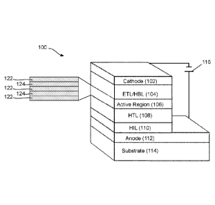
The multiple-QD-layer QLED device 100 comprises a plurality of layers 102 to
112 of different materials sequentially coupled together and to a substrate
114 (or
otherwise deposited thereto). In particular, the multiple-QD-layer QLED device
100 in
these embodiments comprises, sequentially named from the substrate 114, an
anode layer
112, a HTL 108, an active emission region 106, an ETL/HBL 104, and a cathode
layer
102. In these embodiments, the anode layer 112 is transparent and the cathode
layer 102
is non-transparent.
13
CA 03074241 2020-01-28
WO 2019/071362
PCT/CA2018/051297
The active emission region 106 comprises a plurality of thin QD layers 122
such
as one (1) to five (5) QD layers 122 interleaved with one or more QB layers
124 such that
each QB layer 124 is sandwiched between a pair of adjacent QD layers 122.
Therefore,
the number of the QD layers 122 is greater than that of the QB layers 124 by
one (1). In
other words, the active emission region 106 comprises n QD layers interleaved
with (n ¨
1) QB layers where n is a positive integer greater than one.
The QB layer 124 is used to decrease electron leakage from the active emission
region 106. In these embodiments, the QB layers 124 also act as wetting
layers. In
experimental physics, a wetting layer is an initial layer of atoms that is
grown on a surface
upon which self-assembled quantum dots or thin films are created.
In the example shown in Ms. 2A and 2B, the active emission region 106
comprises three (3) QD layers 122 interleaved with two (2) QB layers 124. Each
QB layer
124 is sandwiched between two adjacent QD layers 122.
QB layers 124 are used for preventing or at least decreasing electron/hole
leakage.
In above embodiments, each QD layer 122 (except the two outermost QD layers
122A and
122B) is sandwiched between an adjacent pair of QB layers 124. The pair of QB
layers
124 retain electrons within the QD layer 122 sandwiched therebetween, and thus
help
increase the concentration of electrons in the QD layer 122.
The QD layer 122A adjacent the ETL 104 does not require any quantum barrier
layer therebetween as the ETL 104 injects electrons into the QD layer 122A and
thereby
electrons would unlikely (i.e., with a small probability) move from the QD
layer 122A into
the ETL 104. The QD layer 122B adjacent the HTL 108 does not require any
quantum
barrier layer therebetween as the HTL 108 acts as an EBL and thereby electrons
would
unlikely move from the QD layer 122A into the HTL 108.
The thickness of the QD layer 122 and that of the QB layer 124 significantly
impact
the performance of the multiple-QD-layer QLED device 100. In some embodiments,
the
thickness of each QD layer 122 is greater than that of each QB layer 124. For
example, in
one embodiment, each QD layer 122 is a thin QD film with a thickness of about
15 nm to
nm. The thickness of each QB layer 124 is about 1 nm to 5 nm. In some
embodiments,
30 the thickness
of each QD layer 122 is preferably about eight (8) times of that of each QB
14
CA 03074241 2020-01-28
WO 2019/071362
PCT/CA2018/051297
layer 124. For example, each QD layer 122 has a thickness of about 15 nm to 35
nm and
each QB layer 124 has a thickness of about 2 nm to 4 nm.
Materials of Various Layers
The various layers 102 to 114, 122 and 124 may be made of any suitable
materials.
For example, the cathode 102 may be made of a suitable non-transparent
material such as
silver (Ag), but may also be made of other suitable non-transparent or
transparent material
such as non-transparent Aluminum (Al), transparent ITO, or the like, in some
alternative
embodiments. The anode 112 may be made of transparent Indium Tin Oxide (ITO),
and
the substrate 114 may be made of a transparent supportive material such as
glass.
The ETL 104 may be an inorganic layer made of Zinc Oxide (ZnO) such as
synthesized ZnO nanocrystals which have a valence band and a conduction band
at 7.5
electronvolts (eV) and 4.2 eV, respectively, thereby suitable for use as the
ETL 104 or a
hole-blocking layer (HBL) for improving the performance of the multiple-QD-
layer
QLED 100.
The HTL 108 may be made of poly(9-vinlycarbazole) (i.e., PVK) which has a
valence band and a conduction band at 5.8 eV and 2.3 eV, respectively. In some
alternative
embodiments, the HTL 108 may be made of PVK and further improved by addition
of
Poly [N,N-bi s(4-butylpheny1)-N,N' -bi sphenylb enzi dine] (i. e. , Poly-TPD).
In some
alternative embodiments, the HTL 108 may be made of N,N-diphenyl-N,N-bis(1-
naphthyl-pheny1)-(1,11-bipheny1)-4,4'-diamine (i.e., NPB),
4,4',4"-tri(N-
carbazoly0triphenylamine (i.e., TCTA),
4,4' -Cy clohexylidenebis [N,N-bis(4-
methylphenyl)benzenamine] (i.e., TAPC), poly-TPD, or a mixture thereof Of
course,
other suitable materials may alternatively be used.
The HIL 110 may be made of poly(3,4-ethylenedioxythiophene) polystyrene
sulfonate (i.e., PEDOT:PSS) which has a band diagram located at 5 eV. A
conductive
polymer such as poly(3,4-ethylenedioxythiophene) doped with poly(styrene
sulfonate)
anions (PEDOT:PSS) is widely used in various organic optoelectronic devices.
PEDOT:PSS is a blend of cationic polythiopene derivative, doped with a
polyanion. Such
polymers exhibit high electrical conductivity and good oxidation resistance
thereby
suitable for electromagnetic shielding. Thus, the polymer film has been found
to possess
CA 03074241 2020-01-28
WO 2019/071362
PCT/CA2018/051297
high transparency throughout the visible light spectrum and even in NIR and
near UV
spectrum regions with virtually 100% absorption from 900 nm to 2,000 nm.
Cadmium Selenide/Zinc Sulfide (CdSe/ZnS) has a valence band and a conduction
band at 6.7 eV and 3.4 eV in vacuum, respectively. In the active emission
region 106, each
QD layer 122 is made of CdSe/ZnS-derived nanoparticles which form a large
number of
QDs for capturing and recombining electrons and holes injected thereinto to
emit photons
or light. As each QD layer 122 has a small thickness of about 15 nm to 35 nm
which is
less than de Broglie wavelength (approximately 50 nm) of the CdSe/ZnS-derived
nanoparticles, the crystal lattice mismatch is reduced thereby improving the
light emission
efficiency.
In these embodiments, each QB layer 124 is made of Poly(methyl methacrylate)
(i.e., PMMA). PMMA has a broad bandgap (see references [22] and [23]) and may
be used
for preventing highly mobile electrons from passing the active emission region
106
without recombination.
The interleaved QD layers 122 and QB layers 124 form an active emission region
106 that electrons cannot escape, thereby leading to the decrement of electron
leakage and
increment of external efficiency. Simulation results (described later) show
that using
interleaved QD layers 122 and QB layers 124 can increase the rate of
recombination since
the conduction band of QB layers 124 are wider than that of the QD layers 122.
Consequently, the probability of recombination of electrons and holes in the
active
emission region 106 increases.
Example
In this example, the multiple-QD-layer QLED device 100 comprises an active
emission region 106 formed by a plurality of CdSe/ZnS QD layers 122
interleaved with
one or more QB layers 124 with each QB layer 124 sandwiched between a pair of
adjacent
CdSe/ZnS QD layers 122. As described above, the multiple QB layers 124
significantly
reduce electron leakage.
In this example, the substrate 114 and anode 112 are made from a patterned ITO-
glass substrate with a sheet resistance of 14-16 Qsq-1, offered by Thin Film
Devices
Incorporated of Anaheim, CA, U. S.A, with the coated ITO as the anode layer
112.
16
CA 03074241 2020-01-28
WO 2019/071362
PCT/CA2018/051297
The HIL 110 is made from poly(ethylenedioxythiophene)/polystyrenesulfonate, Al
4083, which is one of the most commonly used PEDOT:PSS formulations offered by
Ossila Ltd of Sheffield, UK.
The HTL 108 is made of PVK with an average molecular weight of 1,100,000
g/mol.
The ETL 104 is formed by synthesized ZnO nanocrystals made from zinc acetate
dehydrate 98%) and potassium hydroxide 85%),
offered by Sigma Aldrich
Corporation of St. Louis, MO, U.S.A.
In this example, ZnO nanoparticles may be prepared by a method reported by
Pacholski et al . (see references [24] to [261) with modifications. According
to the modified
method, 2.46 grams (g) of Zn(Ac)2-2H20 is dissolved in 55 milliliters (ml) of
methanol
at 60 C for 30 minutes. Then, 25 ml of a methanol solution containing 0.96 g
of KOH
(potassium hydroxide) is added dropwise at 60 C while stifling constantly. The
reaction
mixture is stirred two hours under Argon (Ar) atmosphere (i.e., an environment
filled with
noble gas of Ar for isolating the reaction mixture from 02) at a constant
temperature of
60 C. The obtained product appears as a white solution with ZnO nanocrystals
therein.
The ZnO nanocrystals are further washed with methanol twice at the speed of
1500 rpm
for 1 minute. To prepare the 20 mg/ml ZnO solution, 200 mg of nanocrystals are
re-
dispersed in 10 ml n-butanol and 200 pi ethanolamine. The solution is filtered
with 0.2 nm
Polyvinylidene difluoride (PVDF) membrane filters before use.
The cathode 102 is made of silver pellets with a purity of 99.99% offered by
R.D.
Mathis Company of Long Beach, CA, U.S.A.
The QD layers 122 are made from CdSe/ZnS/octadecylamine (630 nm, quantum
yield (QY) >40%) offered by NN-LABS, LLC of Fayetteville, AR, U.S.A.
The QB layers 124 are made from PMMA with an average molecular weight
of 120,000 g/mol.
With above-described materials, the multiple-QD-layer QLED device 100 may be
fabricated via the following fabrication process.
17
CA 03074241 2020-01-28
WO 2019/071362
PCT/CA2018/051297
The substrate 114 may be sonicated in soap bath and rinsed with suitable
purified
water and ethanol. The purified water may be made of any suitable water-
purification
technology such as reverse osmosis (RO). After rinsing, the substrate may be
emerged in
isopropanol bath and sonicated for 5 minutes in a warm sonic bath. For the
hydrophilic
surface treatment, the substrate may be sonicated in fresh 10 vol.% NaOH
solution for 5
minutes in the warm sonic bath and rinsed twice in hot water and finally dried
by blowing
N2 gas.
PEDOT:PSS may be filtered with a rubber-free syringe through a 0.45 p.m PVDF
membrane filter. Then, the filtered PEDOT:PSS is spin-coated onto the pre-
cleaned ITO-
substrate at 3000 rpm for 60 seconds followed by baking at 150 C for 30
minutes, thereby
forming the HIL 110.
To form the HTL 108, PVK may be dissolved in chlorobenzene with a
concentration of 10 mg/ml and spin-coated onto the HIL 110 at 3000 rpm for 60
seconds
and baked at 150 C for 30 minutes.
To form each QD layer 122, CdSe/ZnS QDs may be dissolved inn-octane (5 mg/me
and spin-coated onto the HTL 108 or the neighboring QB layer 124 at 1000 rpm
for 45
seconds followed by annealing at 110 C for 5 minutes. Each CdSe-ZnS QD layer
122 has
a thickness of about 25 nm.
To form each QB layer 124, PMMA may be dissolved in acetone (100 ii.g/m1) and
spin-coated on the neighboring QD layer 122 at 2000 rpm for 45 seconds
followed by
annealing at 110 C for 5 minutes. Each PMMA QB layer 124 has a thickness of
about 3
nm.
In this example, three CdSe/ZnS QD layers 122 interleaved with two PMMA QB
layers 124 are formed.
After forming the active emission region 106 (i.e., the interleaved QD layers
122
and QB layers 124), ZnO nanoparticles obtained as described above may be
dispersed in
a 20 mg/ml (n-butanol) solution and then spin-coated onto the "topmost" QD
layer 122 at
3000 rpm for 50 seconds followed by baking at 60 C for 30 minutes, thereby
forming an
ETL 104 with a thickness of about 90 nm.
18
CA 03074241 2020-01-28
WO 2019/071362
PCT/CA2018/051297
The "top" Ag cathode layer 102 may be deposited onto the ETL 104 by thermal
evaporator with a power of 20W, a pressure of 2x10⁻⁶ mbar and a deposition
time of 25
minutes thereby forming a cathode layer 102 of about 100 nm. The multiple-QD-
layer
QLED device 100 is then formed.
As shown in FIG. 3, the multiple-QD-layer QLED device 100 fabricated as above
has a structure of glass as the substrate 114, ITO as the anode 112, PEDOT:PSS
as the
HIL 110, PVK as the HTL 108, interleaved CdSe-ZnS layers (each about 25 nm
thickness,
as the QD layers 122) and PMMA layers (each about 3 nm thickness, as the QB
layers 124)
forming the active emission region 106, ZnO (about 90 nm thickness) as the ETL
104, and
Ag (about 100 nm thickness) as the cathode 102. By coupling the multiple-QD-
layer
QLED device 100 to a Direct-Current (DC) power source 116, the multiple-QD-
layer
QLED device 100 emits light from its anode side.
As shown in FIG. 4, the multiple-QD-layer QLED device 100 may be tested using
a LED measurement system 130 comprising an integrating receptor 132 (2x2x2
inches
with a 5/8-inch input port) having a sample holder 134 (see FIGs. 5A to 5C)
for holding
the multiple-QD-layer QLED device 100. A Black-Comet spectrometer 136 for UV-
to-
visible spectrum (190 nm to 850 nm) is coupled to the integrating receptor 132
via a F600-
VISNIR fibre optic cable 138 offered by StellarNet Inc. of Tampa, FL, U.S.A.
for
measuring the total power (Watts and Lumens) and Color Rendering Index (CRI)
(see
reference [27]) with measurement results sent to a computing device 140. The 1-
V
characteristic (i.e., the Current¨voltage characteristic or the I-V curve) of
the multiple-
QD-layer QLED device 100 is measured using a Keithley 2400 SourceMeter 142
offered
by Tektronix, Inc. of Beaverton, OR, U.S.A.
FIG. 6A is a flat-band energy level diagram of the multiple-QD-layer QLED
device 100. FIG. 6B is a scanning electron microscope (SEM) image showing the
cross-
section of the multiple-QD-layer QLED device 100.
In most QLEDs. PEDOT:PSS is frequently used for the HIL due to its deep work
function and provides efficient hole injection to the active layer (see
reference 28]).
Deploying a HTL to move away from the injection interfaces, can be very
useful. PVK
energy levels match those of the active layer which makes it a good candidate
for a HTL
(see reference 11291). Also, PVK has a higher valence band compared to
CdSe/ZnS
19
CA 03074241 2020-01-28
WO 2019/071362
PCT/CA2018/051297
nanoparticles (see references [30] and [311). This facilitates the injection
of electrons and
holes to the adjacent layer. CdSe/ZnS QD nanoparticles are widely used as an
active layer
for QLEDs due to their simple synthesis methods, QY efficiency and wide range
of
tunibility (see references [32] to [361). Moreover, inorganic ZnO nanocrystals
are
commonly used as ETLs due to their high electron mobility and matched energy
level
compared to that of adjacent active layer (see references [21] to [231). In
addition, the thick
film of ZnO nanoparticles can serve as a protective layer for QDs during the
deposition of
Ag (see references [41] to [44]). FIG. 6A shows that ZnO nanoparticles are in
favor of
electron transport due to its similar lowest unoccupied molecular orbital
(LUMO) level
with the conductive band of QDs.
One of the major drawbacks of the conventional QLEDs is the efficiency droop
caused by electron leakage (see references [12] and [131). Electron leakage
occurs when
highly mobile electrons cannot recombine with holes due to the difference in
the mobility
of holes and electrons (see reference [151). The hole mobility of PVK is 2.5x
10-6 cm2.V-
1.s-1 (see references [45] and [461) and electron mobility of ZnO is 1.0x10⁻³
cm2.v-1.s-1 for
thin films (see reference [16]). This leads to inefficient injection of charge
at the active
layer resulting in a lower rate of radiative recombination.
Therefore, a good candidate for the quantum barriers must have three
properties:
First, the electron mobility and hole mobility of the polymer should be high
enough to
work as a bridge, letting electrons and holes pass efficiently. Second, in
order to prevent
electrons from passing without radiative recombination, the conductive band of
the QB
layer 124 should be significantly higher than the conductive band of the QD.
Third, the
QB layer 124 should have higher energy at the valence band compared to the QD
such that
holes can pass through the QD layer without facing a large energy gap. If the
quantum
barrier satisfies these conditions, electrons will face a significant energy
barrier when
passing the active layer, which leads to a higher concentration of electrons
at the active
layer (see references [22] and [23]).
Thin film of PMMA possesses the above-mentioned energy bandgap properties,
which makes it a strong candidate for QB layers 124. Moreover, using PMMA with
acetone as a solvent for forming the QB layers 124 would not wash or remove
the
CdSe/ZnS dissolved in octane. Therefore, in some embodiments, it is preferable
to use
CA 03074241 2020-01-28
WO 2019/071362
PCT/CA2018/051297
PMMA as the QB layers 124. Conventional QLED fabrication methods/processes may
be
used for fabricating the multiple-QD-layer QLED device 100 in these
embodiments.
As PMMA is an insulator polymer, each spin-coated PMMA QB layer is required
to have a small or thin thickness such that it would not block the current.
Ismael et al . have
shown that by reducing the thickness of PMMA layer, the conductivity increases
significantly (see reference 11491). In this example, each CdSe/ZnS QD layer
122 has a
thickness of about 25 nm, and each PMMA QB layer 124 has a thickness of about
3 nm.
In the SEM image shown in FIG. 6B, the PMMA QB layers 124 (indicated by the
dark
lines) are hardly visible because the adjacent QD layers 122 obstructs the
imaging of the
PMMA QB layers 124.
In some alternative embodiments, thin layers of hole-transport polymers with
above-mentioned energy bandgap properties, such as PVK, TAPC, and Poly-TPD
(see
references [15], [20], [47], and [481), may be used as the QB layers 124.
However, a
drawback of using these polymers as the QB layers 124 is that the
corresponding
fabrication process of the multiple-QD-layer QLED device 100 may be difficult
as most
of these polymers may contain benzene solvents which may cause the removal or
wash-
off of the underlying QD layer 122. One may form the QD layers with a
thickness greater
than required, for compensating possible wash-off and carefully control the
fabrication
conditions when forming the QB layers 124 to control the wash-off to the QD
layers 122.
However, such a process may be difficult.
Alternatively, one may use other suitable QD materials with above-described QB
materials. Examples of QD materials include materials using CdSe, CdTe, CdS,
or InP as
core and using ZnS, ZnSe, ZnTe, CdS, CdSe,CdTe, PbS, PbSe, PbTe, or InAs as
shell.
Experiment and Simulation Results
FIGs. 7A to 7C show the experiment results of different multiple-QD-layer QLED
devices 100 and conventional QLED devices. In these figures, Bn represents a
multiple-
QD-layer QLED device 100 having an active emission region 106 comprising n
CdSe/ZnS
QD layers 122 interleaved with (n ¨ 1) PMMA QB layers 124 fabricated as
described
above, where n = 2, 3, 4, 5, , and An represents a conventional QLED device
having a
21
CA 03074241 2020-01-28
WO 2019/071362
PCT/CA2018/051297
single CdSe/ZnS QD layer with a thickness about or equal to the total
thickness of the QD
layers 122 of Bn but with no QB layers.
FIG. 7A shows a comparison of output powers of the multiple-QD-layer QLED
devices 100 at a voltage of 8 volts (V). The multiple-QD-layer QLED devices
100 in this
comparison have n QD layers 122 interleaved with (n ¨ 1) PMMA QB layers 124
fabricated as described above, where n = 2, 3, 4, or 5. As can be seen, the
multiple-QD-
layer QLED device 100 having three (3) QD layers 122 interleaved with two (2)
PMMA
QB layers 124 (i.e., B3) exhibits the largest power output. It is known that
using PMMA
with acetone as the solvent can reduce the roughness of the underlying layers
(see
reference [161). Moreover, more layers may cause more dislocations and traps
propagating
in the active emission region. Therefore, with the increase of the number of
PMMA QB
layers 124 to more than four layers, the efficiency of the multiple-QD-layer
QLED device
100 may significantly decrease. Blue shifting effects also become dominant
when four
PMMA QB layers 124 are used due to large energy band gap of the QB layers.
FIG. 7B shows a comparison of output powers of a multiple-QD-layer QLED
device B3 and a conventional QLED device A3 at a voltage of 8 V. The multiple-
QD-layer
QLED device B3 has an active emission region 106 comprising three CdSe/ZnS QD
layers 122 interleaved with two PMMA QB layers 124. The conventional QLED
device
A3 has a CdSe/ZnS QD layer with a thickness about or equal to the total
thickness of the
three CdSe/ZnS QD layers 122 of B3 but with no QB layers. As shown, the
multiple-QD-
layer QLED device B3 has a power output significantly larger than that of the
conventional
QLED device A3. In particular, the peak of B3 is 1.88 times of that of A3.
The significantly greater output-power of the multiple-QD-layer QLED device B3
shows that interleaved QB layers 124 significantly increases the concentration
of electrons
at the active layer at 8 V.
Moreover, those skilled in the art will appreciate that an increased thickness
of a
CdSe/ZnS QD layer may cause severe lattice mismatch and may subsequently cause
an
increased number of dislocations and defaults. Such dislocations and defaults
may lead to
trap spots for electrons and holes thereby increasing non-radiative
recombination and
lowering efficiency (see reference [52]).
22
CA 03074241 2020-01-28
WO 2019/071362
PCT/CA2018/051297
Therefore, by substantially dividing the thick CdSe/ZnS QD layer of ,43 into a
plurality of thin QD layers 122 of B3, lattice mismatch and energy traps in
each thin
CdSe/ZnS QD layer 122 in B3 are reduced which in turn leads to increased
radiative-
recombination and increased output-power.
FIG. 7C shows the current density versus voltage characteristics of B3 and A3
with
the insert showing the CIE (Commission Internationale de l'Elcairage) color
coordinates
of B3. The current densities of B3 and A3 dramatically increase (e.g., to 0.02
mA/mm2
which causes the QLED devices B3 and .43 to emit light at a visible light
strength) when
the voltage reaches 3.5 V and 2 V, respectively. The operating voltage of B3
is higher than
A3 which may be due to the presence of non-conductive PMMA QB layers 124 in
the
active emission region 106. Moreover, the wide energy bandgap of PMMA also
implies
high voltages to start the injection of excitons. Compared to B3, the
conventional QLED
device A3 does not have any PMMA QB layers and requires lower voltages to turn
on.
The symmetric emission peak at 638 nm with a narrow full-width at half-maximum
of 34.7
nm corresponds to the CIE color coordinates of (x=0.677, y=0.295), which are
close to the
spectral locus and preferable for display applications.
Table 1 shows a comparison ofA3 and B3 in terms of operating voltage, full
width
at half maximum (FWHM) and efficiency. As shown, B3 has a higher operating
voltage
as the PMMA QB layers 124 require higher driving voltage for a operating
current.
FVVHMs ofA3 and B3 are in the range of 35 nm to 40 nm thereby promising for
pure color
emissions (see reference [53]). The presence of the PMMA QB layers 124 in B3
increases
the current efficiency from 6.7 Cd/A to 19.0 Cd/A, increases power efficiency
from 2.6
Lm/W to 7.5 Lm/W and increases luminescent from 111,000 Cd/m2 to 207,000
Cd/m2.
23
CA 03074241 2020-01-28
WO 2019/071362
PCT/CA2018/051297
Table. 1 Comparing Current efficiency and Power efficiency of A3 and B3.
Sample A3 B3
Operating Voltage (V) 6 6.6
Testing Voltage (V) 8 8
FWHM (nm) 34.6 37.4
Current (mA) 148 98
Luminescent (Cd/m2) 111,000 207,000
Current Efficiency (Cd/A) 6.7 19
Power Efficiency (Lm/W) 2.6 7.5
Active Layer QD/QD/QD QD/PMMA/QD/PMMA/QD
Simulations of the multiple-QD-layer QLED device 100 are conducted using
APSYS, a software package of the Advanced Physical Models of Semiconductor
Devices
offered by Crosslight Software Inc. of Vancouver, BC, Canada (see reference I-
541), for
determining the optimal number of PMMA QB layers 124 for enhancing the
radiative
recombination rate. In the simulations, The CdSe/ZnS over PMMA band offset
ratio is
considered to be 0.75. The properties of PMMA are defined based on the
reference 1,551.
In the simulations, the electron and hole concentrations at the active layer
under a bias
voltage are studied.
FIG. 8A shows a finite element method (FEM) structure of the multiple-QD-layer
QLED device B3 in APSYS. In particular, the FEM structure used in the
simulation
comprises a 50 nm Hole Injection Layer with number of positive doped particles
of about
5x10²³ m-3, a 50 nm Electron Injecting Layer with number of negative doped
particles of
about 5x10²³ M-3, an active emission region 106, and a 50 nm Electron
Transport Layer.
The active emission region 106 comprises three CdSe/ZnS QD layers interleaved
with two
PMMA QB layers 124. Each CdSe/ZnS QD layer has a thickness of 8 nm, and each
PMMA QB layer 124 has a thickness of 1 nm. It is noted that the structure
(except the
24
CA 03074241 2020-01-28
WO 2019/071362
PCT/CA2018/051297
active emission region 106) shown in FIG. RA is used for simulation and is
different to
that shown in FIG. 3 (which is used for experiments). However, as the testing
and analysis
below are focused on the active emission region 106, the structure difference
outside the
active emission region 106 does not significantly affect the testing and
analysis results of
the active emission region 106.
As a first step, the QD material is defined in APSYS as an embedded material
inside a quantum-barrier region, and the properties of the QD material are
identified. Next,
the structure of the QD layers 122 is defined using a separate sub-project,
and the
properties of the QD layers 122 are loaded back into the main macroscopic
simulation.
Quantum levels and optical transition overlaps from microscopic solutions
calculated from
this part are then imported to the main simulation as input.
After defining the simplified FEM structure of the multiple-QD-layer QLED
device 100, the initial state of the simulation is set to the equilibrium
state which includes
two conditions: (i) there exists no external bias and (ii) the device is under
thermal
equilibrium. Therefore, the voltage and current on all electrodes are zero.
The scan statement is used by the main simulator engine to activate the
equation
solver while only the voltage of contacts is changing, and the current is
being calculated.
This is done by slowly modifying a previously known solution and gradually
updating the
control variables such as the current. An updated solution is then found using
a non-linear
Newton algorithm with the previously known solution as the initial guess.
After
convergence is achieved, the solver continues to update the solution until the
defined
maximum voltage (3.4 V) has been reached. The voltage of 3.4 V is chosen as
the target
voltage based on the simulation curve
results. The output of the software is visualized
by using CrosslightView software.
As a comparison, FIG. RB shows a FEM structure of the conventional QLED
device A3 in APSYS which comprises a single CdSe/ZnS QD layer with a thickness
equal
to the total thickness of the CdSe/ZnS QD layers 122 of B3 and does not
comprise any QB
layers.
FIG. 9A illustrates the Photoluminescence (PL) intensities of four multiple-QD-
layer QLED devices B2, B3, B4, and BS at 3.4 V. As shown, the multiple-QD-
layer QLED
device B3 (three QD layers 122 interleaved with two QB layers 124) produces
the
CA 03074241 2020-01-28
WO 2019/071362
PCT/CA2018/051297
maximum PL intensity, which is consistent to the experimental results shown in
FIG. 7A.
While FIG. 7A shows that B4 has a higher power-output peak than B2, FIG. 9A
shows
that B2 has a higher PL-intensity peak than B4.
FIG. 9B shows the PL intensities of a multiple-QD-layer QLED device B3 and a
conventional QLED device A3 at 3.4 V. As shown, the multiple-QD-layer QLED
device
B3 (three QD layers 122 interleaved with two QB layers 124) exhibits a PL-
intensity peak
about 1.79 times of that of the conventional QLED device A3, which is
consistent to the
results shown in FIG. 7B.
FIG. 9C shows the density-voltage (J-V) characteristics of the multiple-QD-
layer
QLED device B3. As shown, the operating voltage of the simulated model of B3
is about
3.4 V.
FIG. 10 shows (a) the electron concentration of a multiple-QD-layer QLED
device
100, (b) the electron concentration of a conventional QLED device (without QB
layers),
(c) the hole concentration of the multiple-QD-layer QLED device 100, and (d)
the hole
concentration of the conventional QLED device, all obtained from the APSYS
simulation.
The thickness of the QD layers in (b) and (d) are equal to the total thickness
of the three
QD layers in (a) and (c). The direction of electron/hole injection is
indicated with arrows.
FIG. 10 is a greyscale image using darkness as the indication of the
concentration of
electrons (for (a) and (b)) and holes (for (c) and (d)). As shown by the
legend of FIG. 10,
darker grey represents higher electron/hole concentration and lighter grey
represents lower
electron/hole concentration.
A comparison of FIG. 10(a) and (b) shows that the presence of two QB layers
124
greatly increases electron concentration, particularly in the first two QD
layers. The same
conclusion is observable when comparing FIG. 10 (c) and (d).
FIG. 11A shows the radiative recombination rates of a multiple-QD-layer QLED
device B3 and a conventional QLED device A3, respectively, relative to
location along a
hypothetical line passing through the active layer on x = 60 ti.m. As shown,
the presence
of QB layers 124 in the active emission region 106 results in a higher photon
emission rate.
The recombination rate calculation was not conducted for layers other than the
QD layers
122 for the purpose of simplicity.
26
CA 03074241 2020-01-28
WO 2019/071362
PCT/CA2018/051297
FIG. 11B shows the normalized maximum PL intensities of multiple-QD-layer
QLED devices Bn and conventional QLED devices An with n = 2, 3, 4, 5, and 6
(i.e., the
numbers k of QB layers are k = 1, 2, 3, 4, and 5) at different voltages (3.4 V
and 5.8 V).
Herein, the 3.4 V voltage is determined by the J-V characteristics of the
multiple-QD-layer
QLED model. As other applications such as lasers may require higher voltages,
the 5.8 V
voltage is also used in the simulation.
As shown, with the operating voltage of 3.4 V, the presence of QB layers 124
in
the multiple-QD-layer QLED devices Bn increases the PL intensity, among which
k = 2
(i.e., B3 having three QD layers interleaved with two QB layers) gives rise to
the largest
normalized maximum PL intensity. At higher voltages such as at 5.8 V, the
multiple-QD-
layer QLED devices Bn also exhibit superior performance in terms of the PL
intensities,
compared to the conventional QLED devices An. At 5.8 V, k = 4 (i.e., B5 having
five QD
layers interleaved with four QB layers) gives rise to the largest normalized
maximum PL
intensity. FIG. 11B also shows that the performance difference between the
multiple-QD-
layer QLED devices Bn and the conventional QLED devices An is greater at
higher
voltages (e.g., 5.8 V) than at lower voltages (e.g., 3.4 V).
The above experiment results and simulation results show that, with PMMA QB
layers interleaved with CdSe/ZnS QD layers, the multiple-QD-layer QLED devices
100
exhibit higher efficiency than conventional QLED devices having a single
CdSe/ZnS QD
layer and without any QB layers. Compared to conventional QLED devices, the
multiple-
QD-layer QLED devices 100 has a lower rate of electron leakage which leads to
a higher
rate of radiative recombination. The multiple-QD-layer QLED device B3 having
interleaved three QD layers 122 (each with a thickness of about 25 nm) and two
QB layers
124 (each with a thickness of about 3 nm) may be an optimized device with a
current
efficiency of 19 cd/A and a luminescent of 207,000 Cd/m2.
Further simulation/experiment results are presented in FIGs. 12 to 21.
FIG. 12 shows the maximum radiative recombination rates of multiple-QD-layer
QLED devices 100 with different numbers n of QD layers 122 and conventional
QLED
devices at 5.8 V, where the results of multiple-QD-layer QLED devices 100 are
obtained
by neglecting the auger recombination and non-radiative recombination. In
other words,
FIG. 12 shows the simulation results of maximum radiative recombination rates
of ideal
27
CA 03074241 2020-01-28
WO 2019/071362
PCT/CA2018/051297
multiple-QD-layer QLED devices 100 in which the QB layers have no defect.
Moreover,
when n = 1, the multiple-QD-layer QLED device 100 is effectively equivalent to
a
conventional QLED device that has a single (thin) QD layer and without any QB
layers.
With the number n of QD layers 122 increasing, the maximum radiative
recombination rate of the multiple-QD-layer QLED device 100 increases. When
the
number of QD layers 122 to five (5) layers, the maximum radiative
recombination rate
reaches an upper bound and further increasing the number n of QD layers would
not lead
to further increase of the maximum radiative recombination rate.
On the other hand, with the increase of the thickness of the single QD layer
(i.e.,
with the increase of n), maximum radiative recombination rate of the
conventional QLED
device decreases.
FIG. 13 shows the radiative recombination in each QD layer 122 of a multiple-
QD-
layer QLED device 100 having five QD layers 122 interleaved with four QB
layers 124.
As a comparison, FIG. 14 shows the radiative recombination in the QD layer of
a
conventional QLED device having a single QD layer and without any QB layers.
FIGs. 15A and 15B show the concentration of electrons in each QD layer 122 of
a
multiple-QD-layer QLED device 100 having five QD layers 122 interleaved with
four QB
layers 124. As a comparison, FIGs. 16A and 16B show the concentration of
electrons in
the QD layer of a conventional QLED device having a single QD layer and
without any
QB layers.
FIG. 17 shows the spontaneous emission rate versus wavelength of a multiple-QD-
layer QLED device 100 at various operating voltages (1 V to 6 V), wherein the
spontaneous emission is also called luminescence and is the process in which a
quantum
mechanical system transitions from an excited-energy state to a lower-energy
state and
emits an energy in the form of a photon. In FIG. 17, the first peak 152 occurs
because of
the existence of QB layers 124 and the second peak 154 is related to quantum
dots.
Moreover, it can be seen that the light emission peak increases with the
increase of the
operating voltage from 1 V to 6 V.
28
CA 03074241 2020-01-28
WO 2019/071362
PCT/CA2018/051297
FIG. 18 shows the total energy produced by the multiple-QD-layer QLED device
100 versus the current intensity. FIG. 18 shows that there is a linear trend
between the total
energy and the current.
FIG. 19 shows the transmitted photons versus the current of a multiple-QD-
layer
QLED device 100. Two factors determine the amount of energy the photon
transmits,
including the initial energy of the photon and its angle of deflection. Each
photon carries
a specific energy related to its wavelength. Therefore, photons of short
wavelength carry
more energy than those of long wavelength. Also, based on the type of
radiative
recombination (direct recombination, Shockley-Read-Hall (SRH) recombination,
or
Auger recombination), transmitted photons change with the current density.
FIG. 20 shows the percentage of transmitted photons versus the current density
of
a multiple-QD-layer QLED device 100. FIG. 20 shows that highest percentage of
transmitted photons in a multiple-QD-layer QLED 100 using CdSe/ZnS as the QD
layers
can be observed at 385 A/m.
FIG. 21 shows the emission/radiation pattern of a multiple-QD-layer QLED
device 100. As shown, the multiple-QD-layer QLED device 100 is substantively a
directional light source with the maximum emitted power in the direction
perpendicular to
the emitting surface. The radiation pattern shown in FIG. 21 indicates that
most of the
energy is emitted within 20 of the direction of maximum light without using
packages
such as plastic lenses to spread or focus the light for a specific angle of
visibility.
Alternative Structure of the QLED Device
In above embodiments, the QLED 100 comprises a HTL 108 adjacent the active
emission region 106 for preventing the non-radiative recombination of holes
and electrons
that may otherwise occur at the interface of the active emission region 106
and the HIL 110.
In some alternative embodiments, the QLED may not comprise any HTL. FIGs.
22A and 22B show the structure of a QLED 300 in these embodiments. FIG. 23A
shows
the structure of the multiple-QD-layer QLED device 300 used in a simulation in
these
embodiments, and FIG. 23B shows the energy level diagram for the layers of the
multiple-
QD-layer QLED device 300.
29
CA 03074241 2020-01-28
WO 2019/071362
PCT/CA2018/051297
As shown, the active emission region 106 is sandwiched between an ETL/HBL
104 and a HIL 110. The active emission region 106 is directly coupled to the
HIL 110.
Similar to the embodiments shown in FIGs. 2A and 2B, the active emission
region
106 in these embodiments comprises n QD layers interleaved with (n ¨ 1) QB
layers where
n is a positive integer greater than one such that each QB layers 124 is
sandwiched between
a pair of adjacent QD layers 122.
Those skilled in the art will appreciate that in various embodiments, the QLED
device 100 or 300 may be manufactured by using any suitable methods for
example,
coating, nanoparticle deposition (such as radio frequency (RF) deposition,
thermal
evaporation deposition or chemical vapor deposition (CVD) method), and/or the
like.
In some alternative embodiments, the above-described multilayer design and
architecture may be applied to some organic light-emitting diodes (OLEDs) for
improving
the efficiency thereof When using the above-described multilayer architecture,
it may be
important to select a suitable type of solvents to ensure that the previous
layers would not
be washed off by PMMA dissolved in acetone.
In some alternative embodiments, the above-described multilayer design and
architecture may be further deployed for fabrication of white QLEDs by coating
colored
(blue/green/red) QD layers between QB layers.
Although embodiments have been described above with reference to the
accompanying drawings, those of skill in the art will appreciate that
variations and
modifications may be made without departing from the scope thereof as defined
by the
appended claims.
CA 03074241 2020-01-28
WO 2019/071362
PCT/CA2018/051297
Acronyms
3D three-dimensional
= .
Ag = Silver
.
Al = Aluminum
.
CBP = 4,4'-bis(carbazol-9-yl)biphenyl
.
CdSe = Cadmium Selenide
.
CdSe/ZnS : Cadmium Selenide/Zinc Sulfide
CIE: Commission Internationale del-Elcairage
CRI - color rendering index
.
CVD = chemical vapor deposition
.
= DC . Direct Current
EBL = electron-blocking layer
.
EL - electroluminescence
.
ETL = electron-transport layer
.
eV = electronvolt
.
FEM = finite element method
.
FWHM - full width at half maximum
.
=
g . gram
HBL = hole-blocking layer
.
= 20 HIL . hole-injection layer
HTL - hole-transport layer
.
IQE = internal quantum efficiency
.
ITO = Indium Tin Oxide
.
LED = light-emitting diode
.
LUMO - lowest unoccupied molecular orbital
.
ml = milliliter
.
= NIR . near infrared
nm = nanometer
.
NPB - N,N'-diphenyl-N,N'-bis(1-naphthyl-phenyl)-(1,1'-
biphenyl)-
.
4,4'-diamine
OLED = organic light-emitting diode
.
PEDOT:PSS : poly(3,4-ethylenedioxythiophene) polystyrene
sulfonate
PETE . polyethylenimine ethoxylated
PL = Photoluminescence
.
31
CA 03074241 2020-01-28
WO 2019/071362
PCT/CA2018/051297
PMMA Poly(methyl methacrylate)
= .
Poly-TPD : Poly [N,N'-bis(4-butylpheny1)-N,N'-
bisphenylbenzidine]
PVDF . Polyvinylidene difluoride
PVK = poly(9-vinlycarbazole)
.
QB = quantum-barrier
.
QD = quantum dot
.
QLED = quantum-dot light-emitting diode
.
QY quantum yield
= .
RF - radio frequency
.
RO = reverse osmosis
.
SEM scanning electron microscope
= .
SRH = Shockley-Read-Hall
.
TAPC - 4,4'-Cyclohexylidenebis[N,N-bis(4-
.
methylphenyl)benzenamine]
TCTA = 4,4',4"-tri(N-carbazolyl)triphenylamine
.
UV = ultraviolet
.
V - volts
.
ZnO Zinc Oxide
= .
ZnS = Zinc Sulfide
.
32
CA 03074241 2020-01-28
WO 2019/071362 PCT/CA2018/051297
References
[11 P. Reiss,
J. Bleuse, and A. Pron, "Highly Luminescent CdSe/ZnSe Core/Shell
Nanocrystals of Low Size Dispersion,- Nano Lett., vol. 2,110. 7, pp. 781-784,
2002.
[2] P. 0. Anikeena, J. E. Halpert, M. G. Bawendi, and V. Bulovic, -Quantum
Dot
Light-Emitting Devices with Electroluminescence Tunabe over the Entire Visibe
Spectrum,- Nano Lett., vol. 9, pp. 2532-2536, 2009.
[3] J. J. Li et al., "Large-scale synthesis of nearly monodisperse CdSe/CdS
core/shell
nanocrystals using air-stable reagents via successive ion layer adsorption and
reaction,- J. Am. Chem. Soc., vol. 125, no. 41, pp. 12567-12575, 2003.
[4] F. Chen et al., "Enhanced Performance of Quantum Dot-Based Light-
Emitting
Diodes with Gold Nanoparticle-Doped Hole Injection Layer," Nanoscale Res.
Lett.,
vol. 11, no. 1, 2016.
[5] Q. Huang et al., "High-performance quantum dot light-emitting diodes
with hybrid
hole transport laver via doping engineering," Opt. Express, vol. 24, no. 23,
p. 25955,
2016.
[6] X. Yang et al., "Highly flexible, electrically driven, top-emitting,
quantum dot
light-emitting stickers," ACS Nano, vol. 8, no. 8, pp. 8224-8231, 2014.
[7] X. I. A. 0. J. In et al., "Efficient light-emitting diodes based on
reverse type-I
quantum dots," vol. 7, no. 12, pp. 9297-9305, 2017.
[8] S. Baskoutas and A. F. Terzis, "Size-dependent band gap of colloidal
quantum
dots," J. Appl. Phys., vol. 99, no. 1, 2006.
[9] N.
Chestnoy, T. D. Harris, R. Hull, and L. E. Brus, "Luminescence and
photophysics of cadmium sulfide semiconductor clusters: the nature of the
emitting
electronic state," J. Phys. Chem., ol. 90, no. 15, pp. 3393-3399, 1986.
[10] C. B. Murray, C. R. Kagan, and M. G. Bawendi, "Synthesis and
Characterization
of Monodisperse Nanocrystals and Close-Packed Nanocrystal Assemblies," Annu.
Rev. Mater. Sci., vol. 30, no. 1, pp. 545-610, 2000.
33
CA 03074241 2020-01-28
WO 2019/071362
PCT/CA2018/051297
[11] H. Zhang et al., "Ultrastable Quantum-Dot Light-Emitting Diodes by
Suppression
of Leakage Current and Exciton Quenching Processes," ACS Appl. Mater.
Interfaces, vol. 8, no. 45, pp. 31385-31391, 2016.
[12] J. Piprek, F. Romer, and B. Witzigmann, "On the uncertainty of the Auger
recombination coefficient extracted from InGaN/GaN light-emitting diode
efficiency droop measurements," Appl. Phys. Lett., vol. 106, no. 10, 2015.
[13] B. Thu et al., "Low turn-on voltage and highly bright Ag-In-Zn-S quantum
dot
light-emitting diodes," J. Mater. Chem. C, vol. 6, no. 17, pp. 4683-4690,
2018.
[14] K. Qasim et al., "Large-Area Quantum-Dot Light Emitting Diode Arrays with
ZnO
Nanoparticles as Electron Transport/Injection Layer," Sci. Adv. Mater., vol.
6, no.
12, pp. 2625-2631, 2014.
[15] J. Pan, J. Chen, Q. Huang, L. Wang, and W. Lei, "A highly efficient
quantum dot
light emitting diode: Via improving the carrier balance by modulating the hole
transport," RSC Adv., vol. 7, no. 69, pp. 43366-43372, 2017.
[16] X. Dai et al., "Solution-processed, high-performance light-emitting
diodes based
on quantum dots," Nature, vol. 515, no. 7525, pp. 96-99, 2014.
[17] Q. Zhang et al., "Enhancing extraction efficiency of quantum dot light-
emitting
diodes by surface engineering,- Opt. Express, vol. 25, no. 15, p. 17683, 2017.
[18] Y. Dong et al., "20.2: Ultra-Bright, Highly Efficient, Low Roll-Off
Inverted
Quantum-Dot Light Emitting Devices (QLEDs)," SID Symp. Dig. Tech. Pap., vol.
46, no. 1, pp. 270-273, 2015.
[19] H. H. Kim et al., "Inverted quantum dot light emitting diodes using
polyethylenimine ethoxylated modified ZnO," Sci. Rep., vol. 5, pp. 1-5, 2015.
[20] Y. Jiang, H. Tang, S. Chen, and H. Kwok, "Optimizing the Balance of Holes
and
Electrons in Inverted Quantum Dot Light-Emitting Diodes by Inserting Electron
Transportation Barrier Layer," SID Tec. Dig., pp. 274-277, 2015.
34
CA 03074241 2020-01-28
WO 2019/071362
PCT/CA2018/051297
[21] G. F. Yang et al., "InGaN / GaN multiple quantum wells on selectively
grown GaN
microfacets and the applications for phosphor-free white light-emitting
diodes,"
Rev. Phys., vol. 1, no. 1800, pp. 101-119,2016.
[22] I. Al - Deen Hussein Ali Al - Saidi and R. Jabar, "Investigation of
Optical
Properties of Solochrome Dark Blue Dye Doped Polymer Films," J. Mater. Phys.
Chem., vol. 5, no. 1, pp. 32-38,2017.
[23] D. I. Son, C. H. You, J. H. Jung, and T. W. Kim, "Carrier transport
mechanisms of
organic bistable devices fabricated utilizing colloidal ZnO quantum dot-
polymethylmethacrylate polymer nanocomposites," Appl. Phys. Lett., vol. 97,
no.
1, pp. 1-4,2010.
[24] C. Pacholski, A. Kornowski, and H. Weller, "Self-assembly of ZnO: From
nanodots to nanorods," Angew. Chemie - Int. Ed., vol. 41, no. 7, pp. 1188-
1191,
2002.
[25] E. A. Meulenkamp, "Synthesis and Growth of ZnO Nanoparticles," J. Phys.
Chem.
B, vol. 102, no. 29, pp. 5566-5572,1998.
[26] S. Dayneko et al., "Effect of surface ligands on the performance of
organic light-
emitting diodes containing quantum dots," Proc. SPIE Vol. 9270, vol. 103, no.
6,
p. 927009,2014.
[27] S. R. Forrest, D. D. C. Bradley, and M. E. Thompson, "Measuring the
Efficiency
of Organic Light-Emitting Devices," Adv. Mater., vol. 15, no. 13, pp. 1043-
1048,
2003.
[28] Z. Li et al., "A low-work-function, high-conductivity PEDOT:PSS electrode
for
organic solar cells with a simple structure," Synth. Met., vol. 210, pp. 363-
366,
2015.
[29] U. Wurfel, A. Cuex as, and P. Wurfel, "Charge carrier separation in solar
cells,"
IEEE J. Photovoltaics, vol. 5, no. 1, pp. 461-469,2015.
CA 03074241 2020-01-28
WO 2019/071362
PCT/CA2018/051297
[30] S. S. Lo, L. Yang, and C. P. Chiu, "ZnO/poly(N-vinylcarbazole) coaxial
nanocables for white-light emissions," J. Mater. Chem. C, vol. 3, no. 3, pp.
686-
692, 2015.
[31] F. Meng et al., "An organic-inorganic hybrid UV photodetector based on a
TiO2
nanobowl array with high spectrum selectivity," RSC Adv., vol. 3, no. 44, pp.
21413-21417, 2013.
[32] V. L. Colvin, M. C. Schlamp, and A. P. Alivisatos, "Light-emitting diodes
made
from cadmium selenide nanocrystals and a semiconducting polymer," Nature, vol.
370, no. 6488, pp. 354-357, 1994.
[33] M. K. Choi, J. Yang, T. Hyeon, and D.-H. Kim, "Flexible quantum dot light-
emitting diodes for next-generation displays," npj Flex. Electron., vol. 2,
no. 1, p.
10, 2018.
[34] B. 0. Dabbousi et al., "(CdSe)ZnS Core¨Shell Quantum Dots: Synthesis and
Characterization of a Size Series of Highly Luminescent Nanocrystallites," J.
Phys.
Chem. B, vol. 101, no. 46, pp. 9463-9475, 1997.
[35] M. Mehrjoo, M. Molaei, and M. Karimipour, "A novel process for synthesis
of
CdSe/ZnS core-shell QDs and their application for the Methyl orange (MO)
degradation," Mater. Chem. Phys., vol. 201, pp. 165-169, 2017.
[36] D. V. Talapin, A. L. Rogach, A. Komowski, M. Haase, and H. Weller,
"Highly
Luminescent Monodisperse CdSe and CdSe/ZnS Nanocrystals Synthesized in a
Hexadecylamine-Trioctylphosphine Oxide-Trioctylphospine Mixture," Nano Lett.,
vol. 1, no. 4, pp. 207-211, 2001.
[37] L. Qian, Y. Zheng, J. Xue, and P. H. Holloway, "Stable and efficient
quantum-dot
light-emitting diodes based on solution-processed multilayer structures," Nat.
Photonics, vol. 5, no. 9, pp. 543-548, 2011.
[38] H. Peng, W. Wang, and S. Chen, "Efficient Quantum-Dot Light-Emitting
Diodes
With 4,4,4-Tris(N-Carbazoly1)-Triphenylamine (TcTa) Electron-Blocking Layer,"
IEEE Electron Device Lett., vol. 36, no. 4, pp. 369-371, 2015.
36
CA 03074241 2020-01-28
WO 2019/071362
PCT/CA2018/051297
[39] J. Kw-ak et al., "Bright and efficient full-color colloidal quantum
dot light-emitting
diodes using an inverted device structure," Nano Left., vol. 12, no. 5, pp.
2362-
2366, 2012.
[40] B. S. Mashford et al., "High-efficiency quantum-dot light-emitting
devices with
enhanced charge injection," Nat. Photonics, vol. 7, no. 5, pp. 407-412, 2013.
[41] W. Wang, H. Peng, and S. Chen, "Highly transparent quantum-dot light-
emitting
diodes with sputtered indium-tin-oxide electrodes," J. Mater. Chem. C, vol. 4,
no.
9, pp. 1838-1841, 2016.
[42] J. Meyer et al., "Transparent inverted organic light-emitting diodes with
a tungsten
oxide buffer layer," Adv. Mater., vol. 20, no. 20, pp. 3839-3843, 2008.
[43] G. Parthasarathy, C. Adachi, P. E. Burrows, and S. R. Forrest, -High-
efficiency
transparent organic light-emitting devices,- Appl. Phys. Lett., vol. 76, no.
15, pp.
2128-2130, 2000.
[44] Y. J. Lee et al., "Development of inverted OLED with top ITO anode by
plasma
damage-free sputtering," Thin Solid Films, vol. 517, no. 14, pp. 4019-4022,
2009.
[45] D. H. Lee, Y. P. Liu, K. H. Lee, H. Chae, and S. M. Cho, "Effect of hole
transporting materials in phosphorescent white polymer light-emitting diodes,"
Org. Electron. physics, Mater. Appl., vol. 11, no. 3, pp. 427-433, 2010.
[46] P. D'Angelo et al., "Electrical transport properties characterization of
PVK (poly
N-vinylcarbazole) for electroluminescent devices applications," Solid. State.
Electron., vol. 51, no. 1, pp. 101-107, 2007.
[47] Q. Sun et al., "Bright, multicoloured light-emitting diodes based on
quantum dots,"
Nat. Photonics, vol. 1, no. 12, pp. 717-722, 2007.
[48] Q. Sun, D. W. Chang, L. Dai, J. Grote, and R. Naik, "Multilayer white
polymer
light-emitting diodes with deoxyribonucleic acid-cetyltrimetylammonium
complex as a hole-transporting/electron-blocking layer," Appl. Phy-s. Lett.,
vol. 92,
no. 25, 2008.
37
CA 03074241 2020-01-28
WO 2019/071362
PCT/CA2018/051297
[49] L. N. Ismail, Z. Habibah, M. H. Abdullah, S. H. Herman, and M. Rusop,
"Electrical
properties of spin coated PMMA for OFETs applications," Int. Conf. Electron.
Devices, Syst. Appl., pp. 333-338, 2011.
[50] B. C. Shekar, S. Sathish, and R. Sengoden, "Spin coated nano scale PMMA
films
for organic thin film transistors," Phys. Procedia, vol. 49, no. 0, pp. 145-
157, 2013.
[51] H. Q. Zhang, Y. Jin, and Y. Qiu, "The optical and electrical
characteristics of
PMMA film prepared by spin coating method," TOP Conf. Ser. Mater. Sci. Eng.,
vol. 87, no. 1, 2015.
[52] G. Venturi et al., "Dislocation-related trap levels in nitride-based
light emitting
diodes," Appl. F'hys. Lett., vol. 104, no. 21, 2014.
[53] S. Reineke, M. Thomschke, B. Ltissem, and K. Leo, "White organic light-
emitting
diodes: Status and perspective," 2013.
[54] "APSYS User's Manual." http://www.crosslight.com, 2005.
[55] Z. T. Huang et al., "Electron transport in solution-grown TIPS-pentacene
single
crystals: Effects of gate dielectrics and polar impurities," Chinese Chem.
Lett., vol.
27, no. 12, pp. 1781-1787, 2016.
38